Method and device for electromagnetic field analysis of circuit board, and circuit board and its design method

a technology of electromagnetic field analysis and circuit board, which is applied in the direction of resistance/reactance/impedence, inductance, instruments, etc., can solve the problems of difficulty in obtaining such characteristics, and difficulty in obtaining conductor patterns that may electromagnetically interfere with each other, so as to shorten the running time of electromagnetic analysis and reduce the time and cost required for designing the circuit board. , the effect of reducing the cost of the circuit board

Inactive Publication Date: 2006-09-28
PANASONIC CORP
View PDF2 Cites 3 Cited by
  • Summary
  • Abstract
  • Description
  • Claims
  • Application Information

AI Technical Summary

Benefits of technology

[0048] In the method and the apparatus for analyzing an electromagnetic field of a circuit board, according to the present invention, after dividing the circuit board into a plurality of areas, results obtained by performing the electromagnetic analysis over each of the divided areas are integrated. This approach can drastically shorten running time of the electromagnetic analysis, and time and cost required for designing the circuit board can be significantly reduced. Further, since the result of the simulation can be obtained quickly, it is easy to give feedback to design of the circuit board, thereby optimizing the design of the circuit board.
[0049] Furthermore, in the circuit board and the method for designing the same, according to the present invention, simulation time of the circuit board including a plurality of layers having conductor patterns in which a plurality of spiral inductance patterns are provided can be drastically shortened, thereby contributing to reduce cost of the circuit board. Further, this result is almost equal to a result obtained by simulation without division, enabling design sufficient for practice use.

Problems solved by technology

In particular, because of EMI (electromagnetic interference) between conductor patterns, it was difficult to obtain such characteristics as initially designed using only designer's experiences.
However, such a conventional circuit board will be quite expensive.
Since the above-mentioned circuit board has a plurality of layers with conductor patterns while downsizing and integrating it densely, the various conductor patterns may electromagnetically interfere with each other.
Designing one circuit board using an EM simulation for many days may increase the cost of the circuit board.
But there must be lines for connecting the devices to each other, resulting in various EMI between the lines or between the lines and the devices.
Therefore, as described above, it is difficult to obtain desired characteristics even after designing for a long time, thereby increasing the cost of the circuit board.

Method used


Image

  • Method and device for electromagnetic field analysis of circuit board, and circuit board and its design method
  • Method and device for electromagnetic field analysis of circuit board, and circuit board and its design method
  • Method and device for electromagnetic field analysis of circuit board, and circuit board and its design method

Examples


embodiment 1

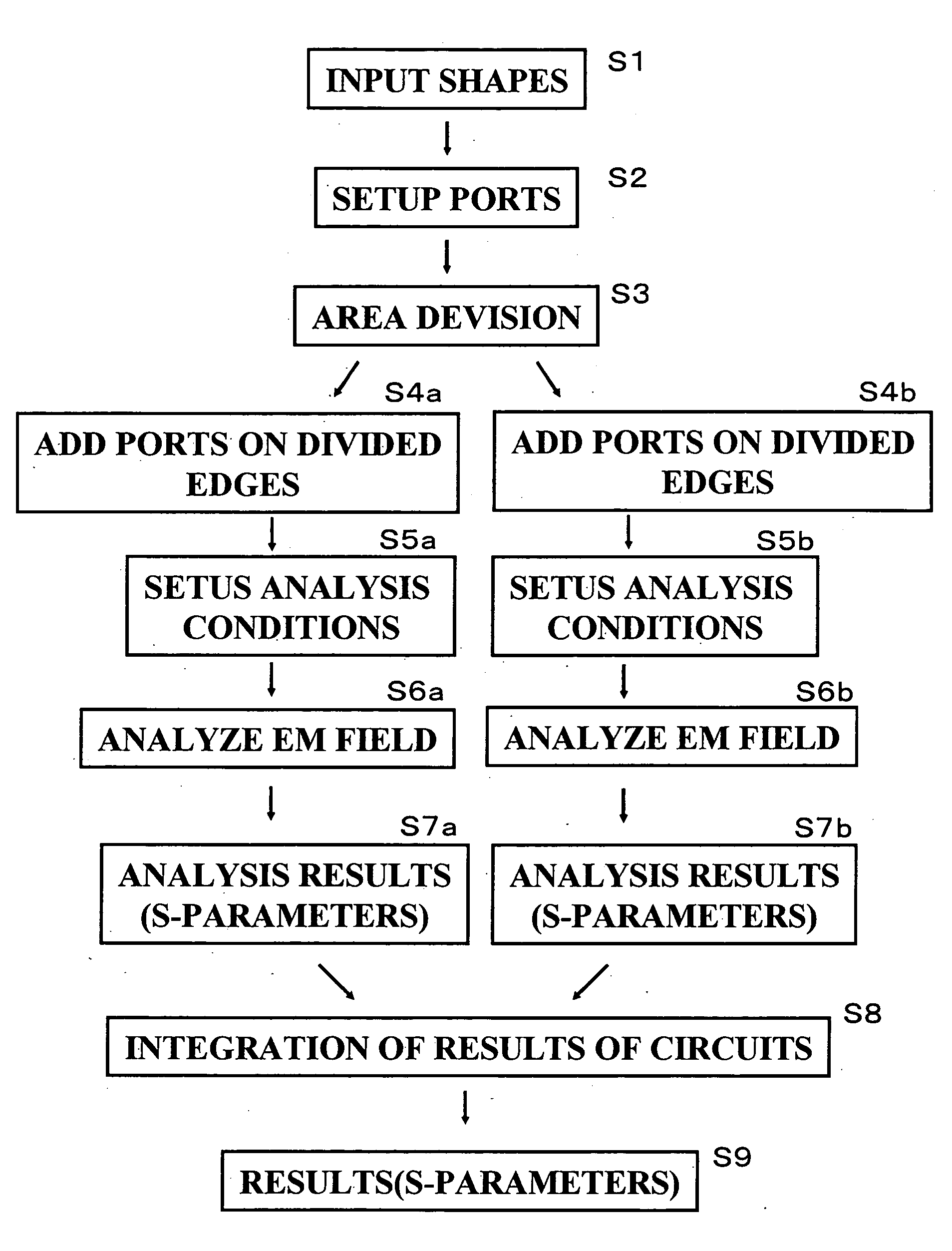
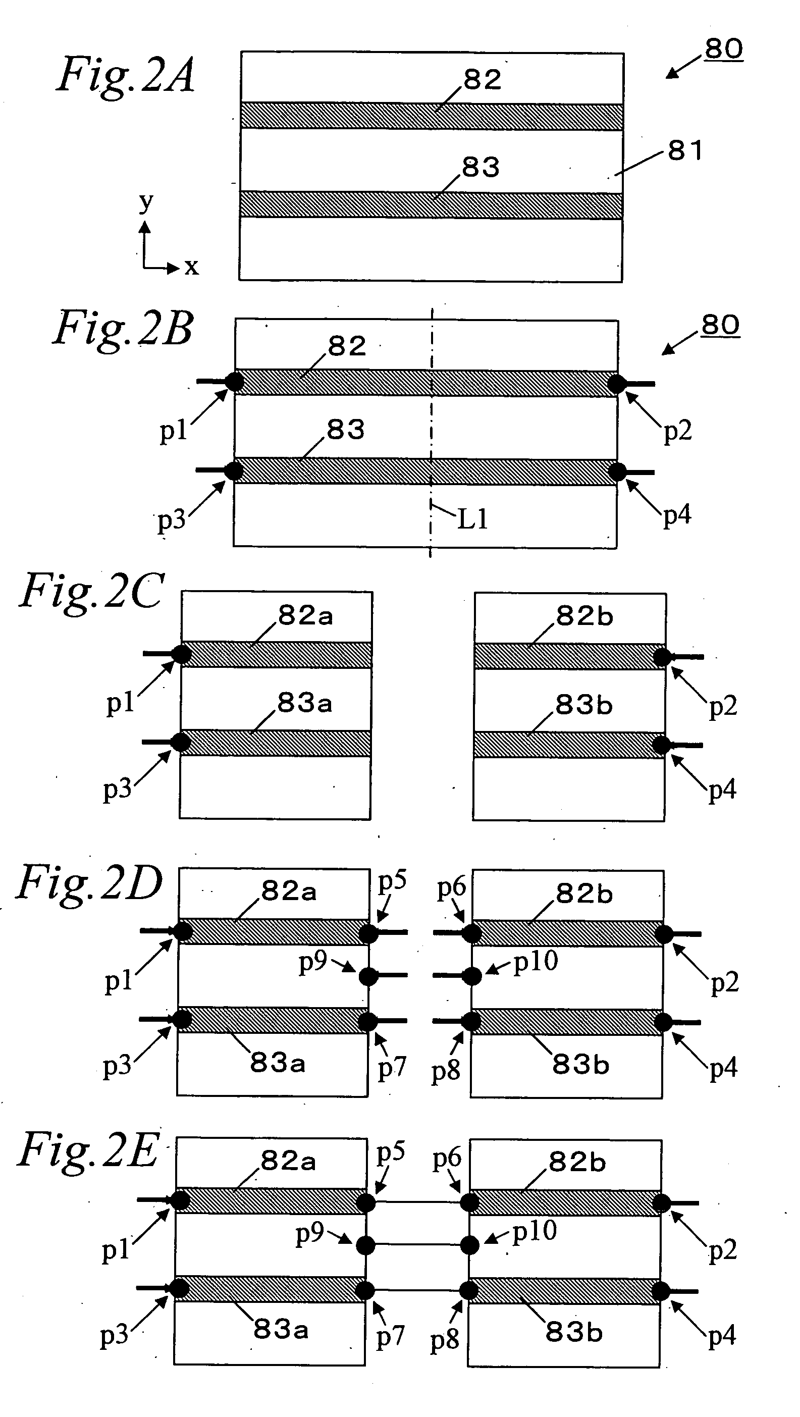
[0082]FIG. 1 is a flowchart showing an example of an electromagnetic simulation according to the present invention. FIGS. 2A to 2E are explanatory views illustrating operation status of the simulation. The EM (electromagnetic) simulator is constituted of a software which can run on a personal computer. The personal computer may include a input device, such as keyboard, a pointing device, such as mouse, a display device, such as liquid crystal display panel, a mass-storage device, such as hard-disk or optical disk, a processing device, such as a micro-processor, and a network device.

[0083] Various data required for the simulation, such as shapes of conductor patterns and signal analysis conditions, can be inputted using the keyboard or the mouse, or from files stored in the mass-storage device, or through a network from another computer. Results of the simulation can be represented on a screen of the display device, or stored in the mass-storage device, or outputted through the netw...

embodiment 2

[0098]FIGS. 3A to 3C are explanatory views illustrating another example of area division in the EM simulation according to the present invention. In this embodiment, operation of the EM simulation is similar to that as described above, but in the step S3 shown in FIG. 1, the multilayer circuit board is divided two-dimensionally into a plurality of areas using dividing lines including a plurality of straight lines parallel to each other.

[0099] For example, as shown in FIG. 3A, the multilayer circuit board 80 is divided by a dividing line L1 which extends straightly along y-direction, like in FIG. 2B, and then, as shown in FIG. 3B, the left divided area is further divided by a dividing line L2 which extends straightly along y-direction, and the right divided area is further divided by a dividing line L3 which extends straightly along y-direction, eventually, into four areas in total. This embodiment exemplifies that the multilayer circuit board is divided into four rectangular areas....

embodiment 3

[0106]FIGS. 4A to 4C are explanatory views illustrating yet another example of area division in the EM simulation according to the present invention. In this embodiment, operation of the EM simulation is similar to that as described above, but in the step S3 shown in FIG. 1, the multilayer circuit board is divided two-dimensionally into a plurality of areas using dividing lines including a plurality of straight lines perpendicular to each other.

[0107] For example, as shown in FIG. 4A, the multilayer circuit board 80 is divided by a dividing line L1 which extends straightly along y-direction, like in FIG. 2B, and then, as shown in FIG. 4B, the left divided area is further divided by a dividing line L4 which extends straightly along x-direction, and the right divided area is further divided by a dividing line L5 which extends straightly along x-direction, eventually, into four areas in total. This embodiment exemplifies that the multilayer circuit board is divided into four rectangul...


PUM

PropertyMeasurementUnit
running timeaaaaaaaaaa
electromagnetic fieldaaaaaaaaaa

Abstract

A method for analyzing an electromagnetic field includes: a step S1 for setting up initial shapes of conductor patterns in each layer of a multilayer circuit board; a step S2 for setting up initial ports for input or output of an external signal in each conductor pattern; a step S3 for dividing two-dimensionally the multilayer circuit board into a plurality of areas; steps S4a and S4b for setting up additive ports on edges of the conductor pattern which has been created by area-division; steps S5a and S5b for setting up individual analysis conditions for the initial ports and the additive ports, respectively; steps S6a and S6b for performing an electromagnetic analysis of the multilayer circuit board by the divided area, based on the analysis conditions; and a step S8 for integrating results of the electromagnetic analysis over each of the divided areas, thereby obtaining results of the electromagnetic analysis over the whole circuit board. By using this approach, an EM analysis of a multilayer circuit board can run quickly to significantly reduce time and cost required for designing the circuit board.

Description

TECHNICAL FIELD [0001] The present invention relates to a method and an apparatus for analyzing an electromagnetic field of a circuit board, which is used in various electronics, and also to a circuit board and a method for designing the same. BACKGROUND [0002] Conventionally, approaches of designing a circuit board using an EM (electromagnetic field) simulation have been made, because a conventional electronics has increasingly required higher accuracy and the circuit board has been configured of a plurality of layers with conductor patterns to downsize and integrate it densely. In particular, because of EMI (electromagnetic interference) between conductor patterns, it was difficult to obtain such characteristics as initially designed using only designer's experiences. Therefore, an analyzing method using an EM analysis simulator has been considered. Conventional EM simulators, such as ADS Momentum supplied by Agilent Technologies, Sonnet supplied by Sonnet, and RF Designer supplie...

Claims


Application Information

Patent Timeline
Patent Type & Authority Applications(United States)
IPC IPC(8): G01R27/00G06F17/50H01F17/00H05K3/00
CPCG06F17/5036H01F17/0013H05K3/0005G06F30/367
Inventor URIU, KAZUHIDEYAMADA, TORUSASAKI, YUKINORI
Owner PANASONIC CORP
Why Eureka
Try Eureka