Semiconductor device

Active Publication Date: 2006-10-05
SEMICON COMPONENTS IND LLC
View PDF4 Cites 18 Cited by
  • Summary
  • Abstract
  • Description
  • Claims
  • Application Information

AI Technical Summary

Benefits of technology

[0009] The present invention was made in consideration of the circumstances described above. A semiconductor device of the present invention includes an isolation region which divides a semiconductor layer into a plurality of element formation regions; an insulating layer formed on the semiconductor layer; and a wiring layer traversing over the isolation region, and wired from one to other one of the element formation regions on a top surface of the insulating layer. The semiconductor device also includes a first conductive plate in the insulating layer under the wiring layer, which is arranged in a manner covering over a junction region between the isolation region and the semiconductor layer, and is electrically connected to the isolation region; and a second co

Problems solved by technology

Therefore, there is the problem that element formation regions are not efficiently arranged with respect to a chip size.
This structure involves a necessity of thickening an insulating film on a top surface of the epitaxial layer, and there is a problem that a higher manufacturing cost i

Method used


Image

  • Semiconductor device
  • Semiconductor device
  • Semiconductor device

Examples


Embodiment Construction

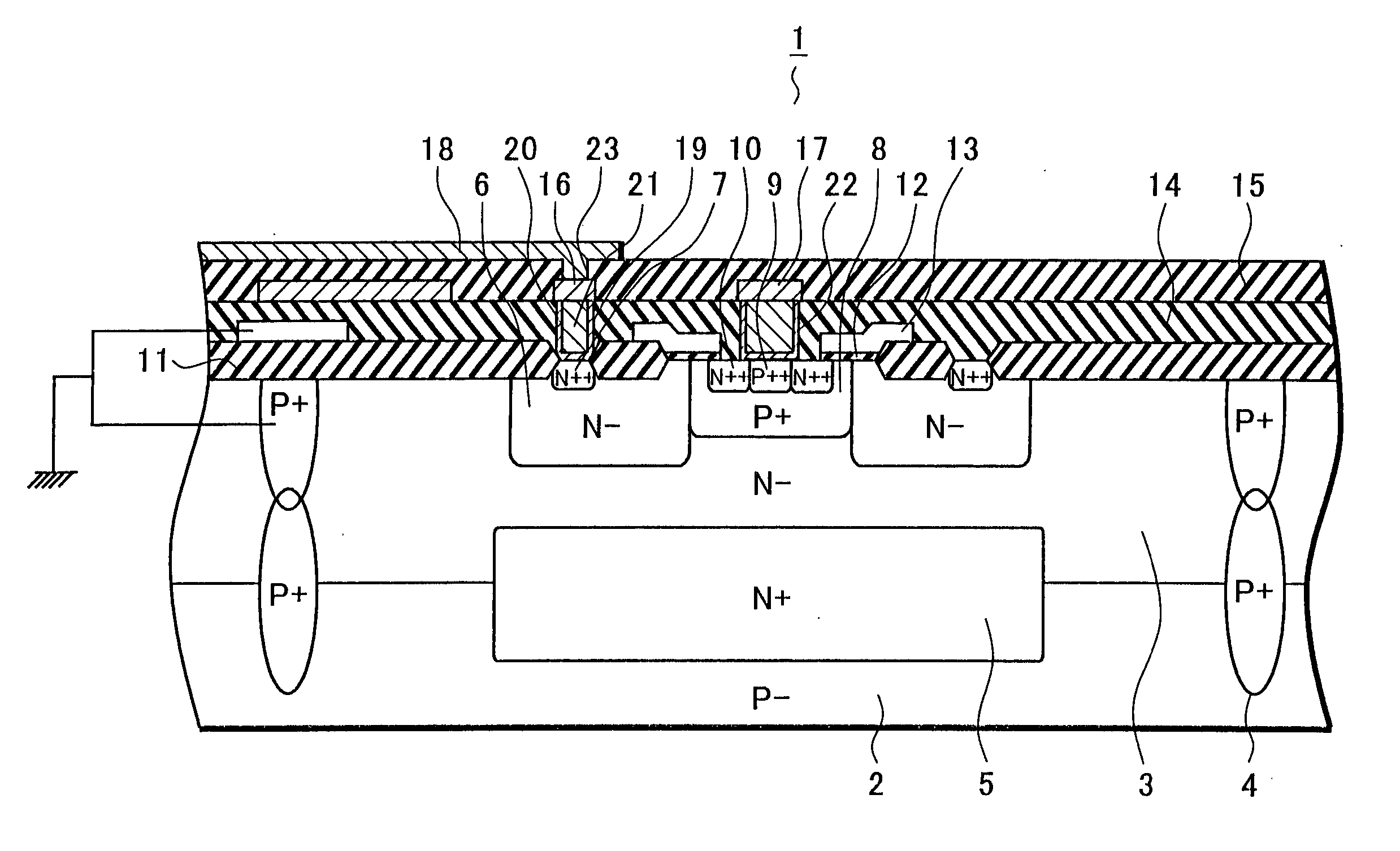
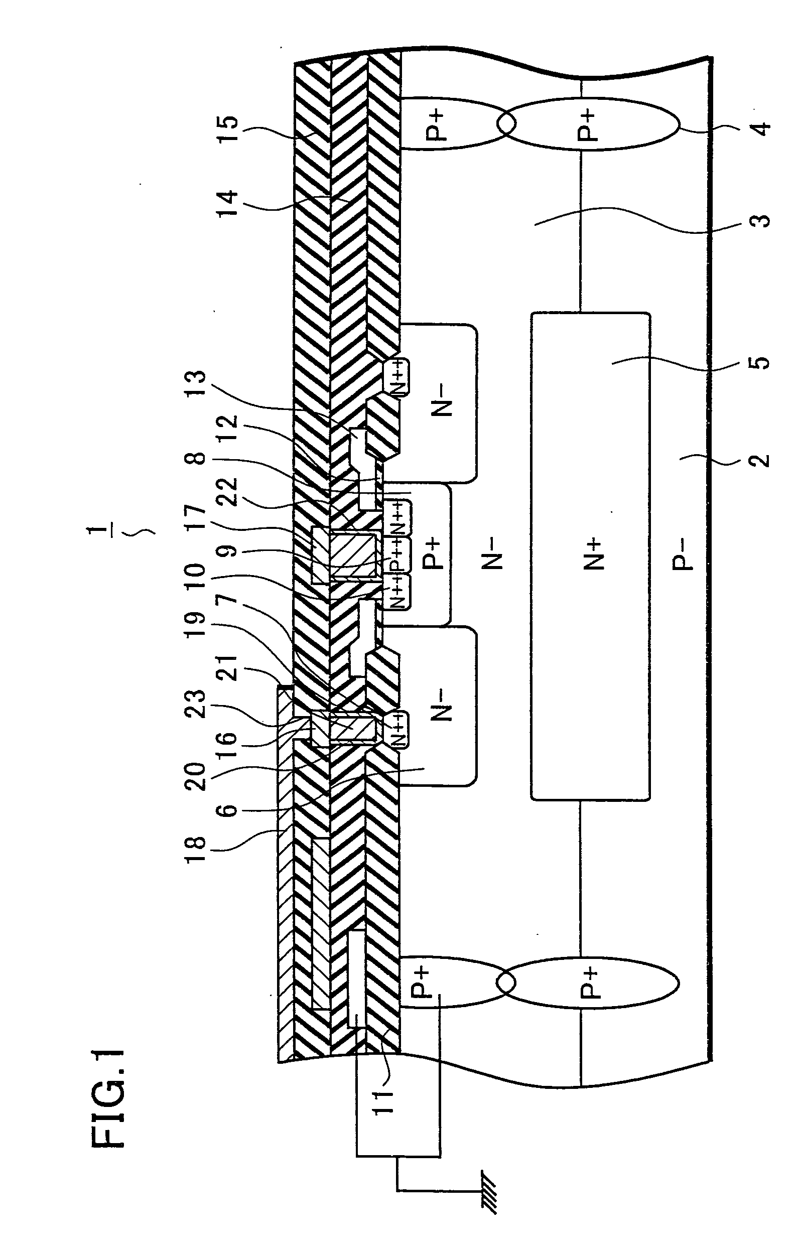
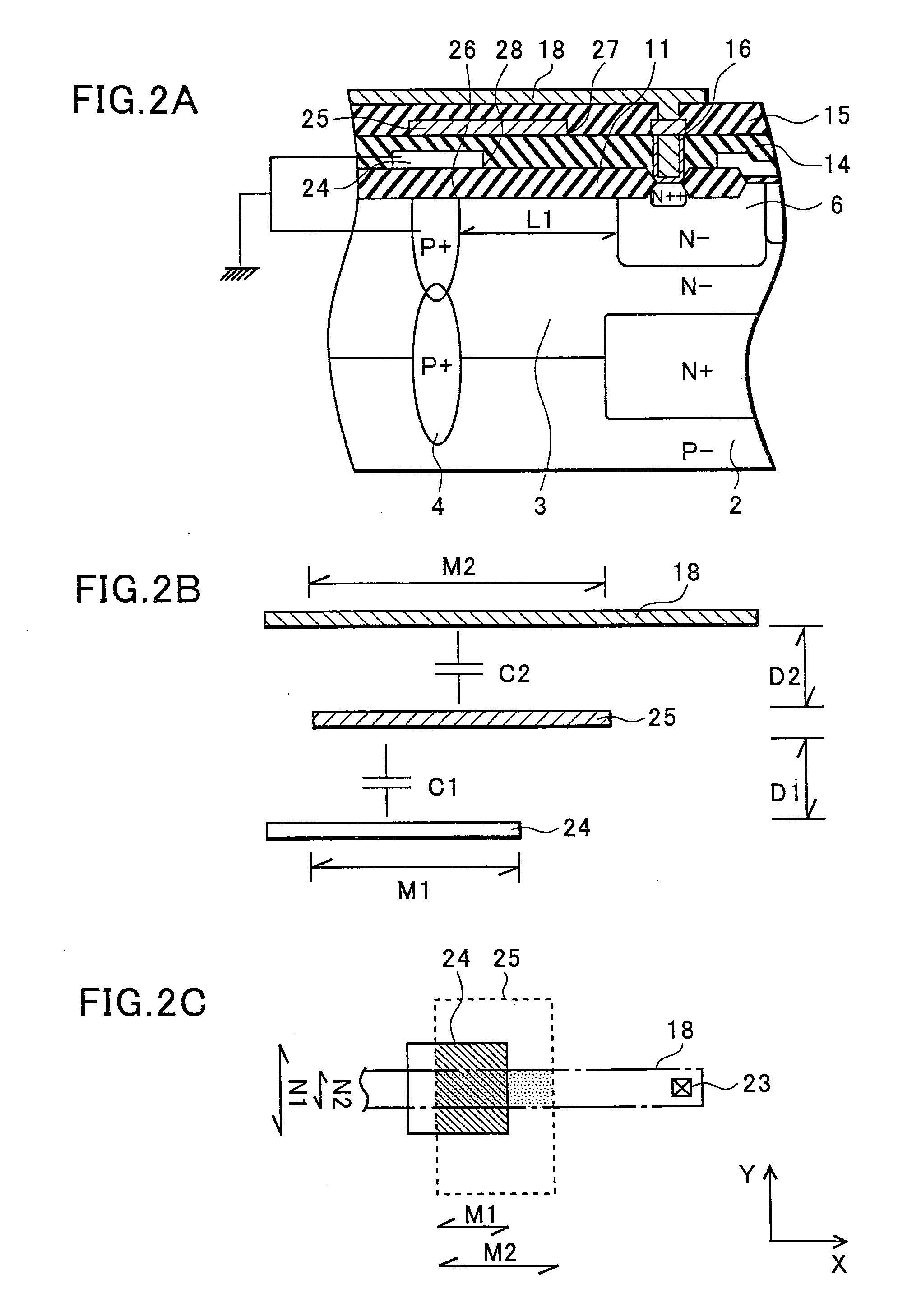
[0024] Hereinafter, a semiconductor device of one embodiment of the present invention will be described in detail with reference to FIGS. 1 to 4B. FIG. 1 is a cross-sectional view for explaining an N-channel LDMOSFET in this embodiment. FIG. 2A is a cross-sectional view for explaining an electric field reduction structure over a top surface of an isolation region in this embodiment. FIG. 2B is as illustration for explaining a state of capacitive coupling over the top surface of the isolation region in this embodiment. FIG. 2C is an illustration for explaining a state of capacitive coupling over the top surface of the isolation region in this embodiment. FIG. 3 is a chart for explaining a relation between a withstand voltage of the LDMOSFET and a ratio of an electric potential of a conductive plate to that of a wiring layer in this embodiment. FIG. 4A is an illustration for explaining an electric potential distribution in the LDMOSFET in this embodiment. FIG. 4B is an illustration fo...


PUM


Abstract

In a conventional semiconductor device, there has been a problem that, in a region where a wiring layer to which a high electric potential is applied traverses a top surface of an isolation region, the withstand voltage is deteriorated. In a semiconductor device of the present invention, an epitaxial layer is deposited on a substrate, and an LDMOSFET is formed in one region divided by an isolation region. In a region where a wiring layer connected to a drain electrode traverses a top surface of the isolation region, a conductive plate having a ground electric potential and another conductive plate in a floating state are formed under the wiring layer. With this structure, electric field is reduced in the vicinity of the isolation region under the wiring layer, whereby a withstand voltage of the LDMOSFET is increased.

Description

Priority is claimed to Japanese Patent Application Numbers JP2005-098966, filed on Mar. 30, 2005, and JP2005-191023, filed on Jun. 30, 2005, the disclosures of which are incorporated herein by reference in its entireties. BACKGROUND OF THE INVENTION [0001] 1. Field of the Invention [0002] The present invention relates to a semiconductor device configured to reduce an electric field concentration in the vicinity of its isolation region and thereby to increase its withstand voltage characteristic. [0003] 2. Background Art [0004] As one of conventional power semiconductor devices, a lateral double diffused metal oxide semiconductor field effect transistor (hereinafter, referred to as an LDMOSFET) has been known. The LDMOSFET is, for example, integrated on the same semiconductor chip as other signal processing circuits are integrated, and used as a driver circuit. There, in one region over a top surface of an isolation region thereof, a drain electrode for applying a high electric poten...

Claims


Application Information

Patent Timeline
IPC IPC(8): H01L29/788
CPCH01L29/0696H01L29/0878H01L29/402H01L29/404H01L29/41725H01L29/42368H01L2924/0002H01L29/456H01L29/7816H01L2924/00
Inventor KIKUCHI, SHUICHIOKAWA, SHIGEAKINAKAYA, KIYOFUMITAKAHASHI, TOSHIYUKI
Owner SEMICON COMPONENTS IND LLC
Why Eureka
Try Eureka