

Semiconductor substrate, substrate for semiconductor crystal growth, semiconductor device, optical semiconductor device, and manufacturing method thereof
a technology for semiconductor crystal growth and semiconductor devices, which is applied in the direction of crystal growth process, semiconductor material growth, semiconductor lasers, etc., can solve the problems of lowering the yield ratio, reducing the yield ratio, so as to achieve the effect of effectively solving the warp of the substrate, improving the yield ratio in manufacturing the semiconductor device by using the semiconductor wafer according to the present invention
- Summary
- Abstract
- Description
- Claims
- Application Information
AI Technical Summary
Benefits of technology
Problems solved by technology
Method used
Image

Examples
first embodiment
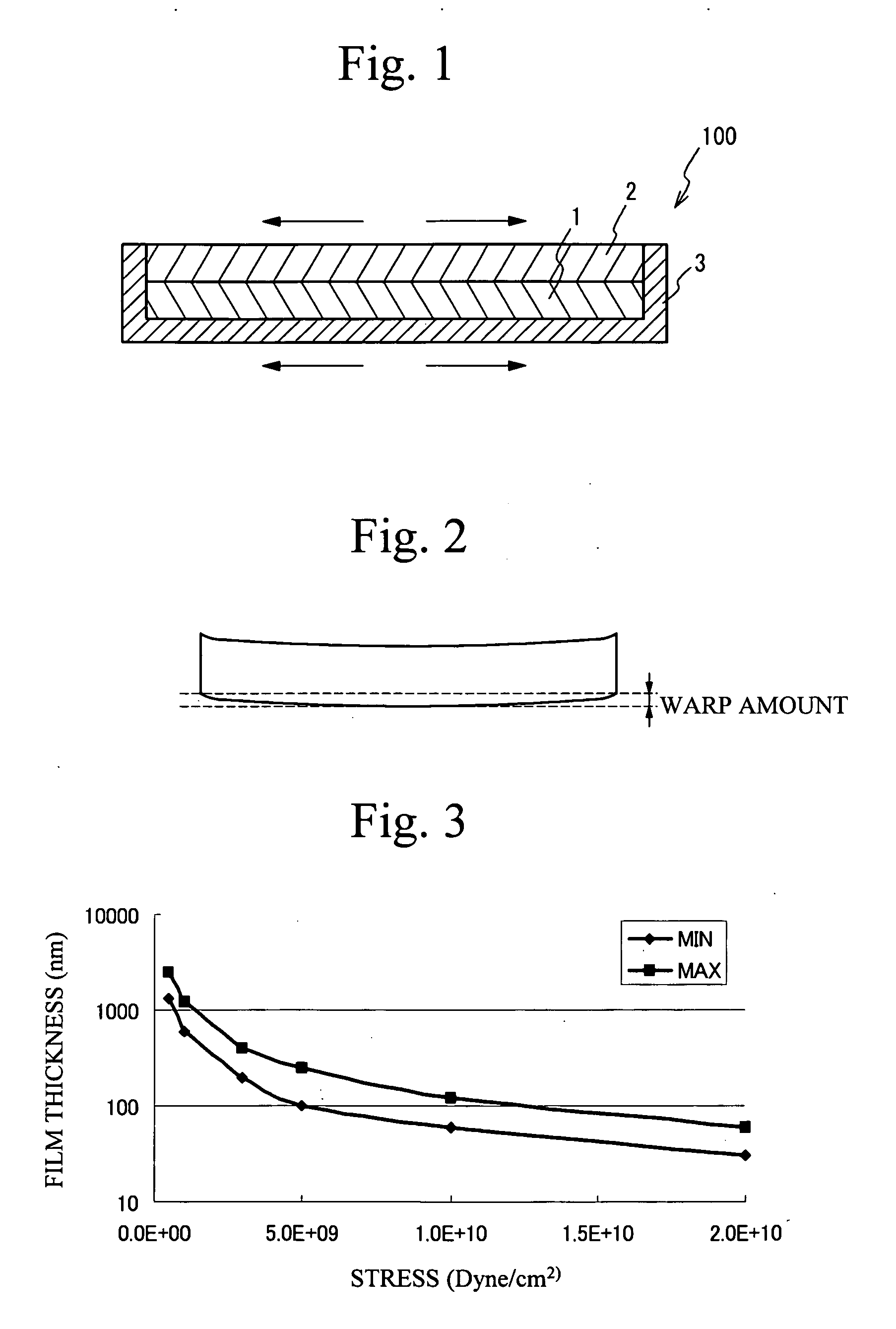
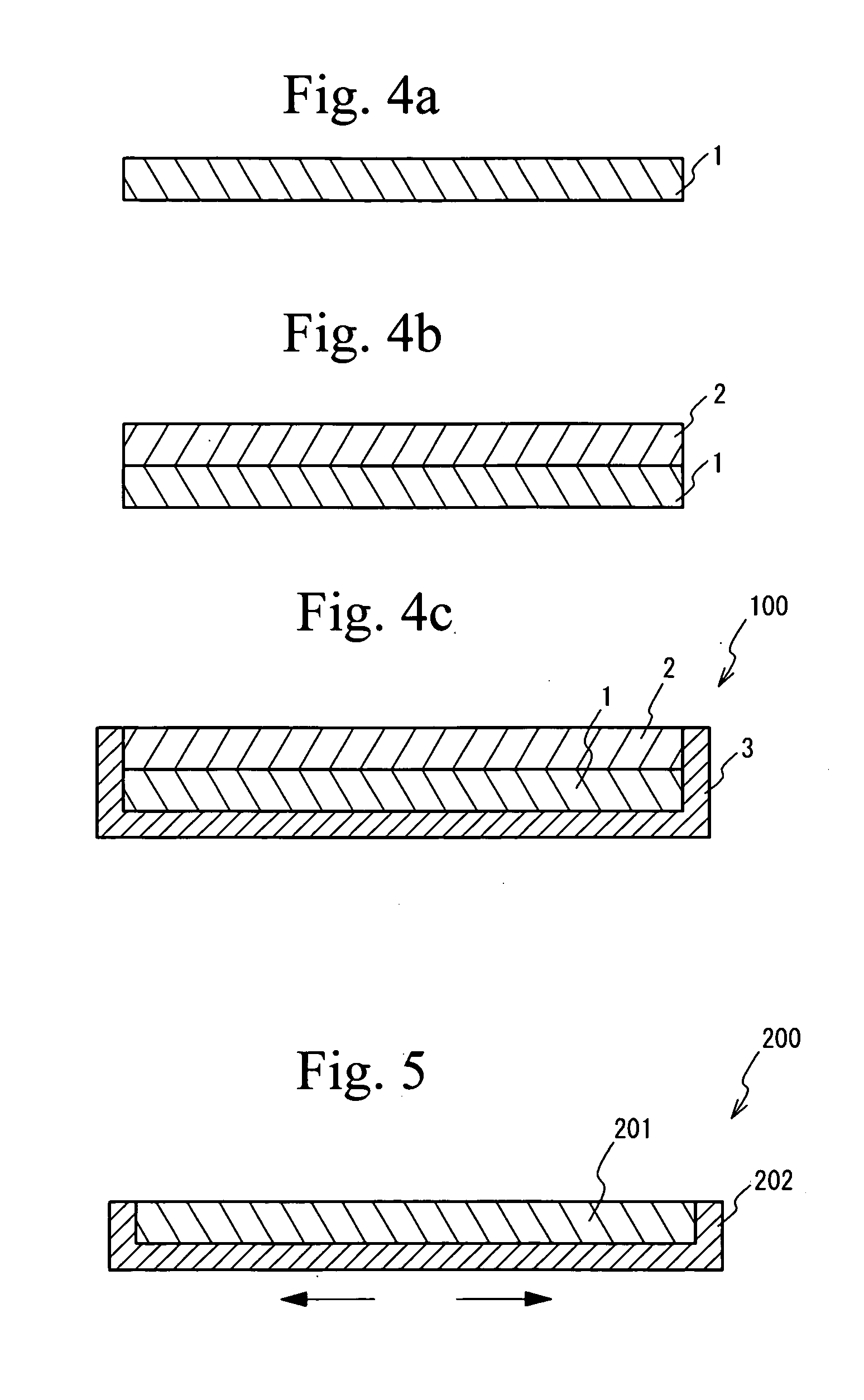
[0038]FIG. 1 shows a typical cross section of a semiconductor substrate 100 according to a first embodiment. As shown in FIG. 1, the semiconductor substrate 100 includes a growth substrate 1, a semiconductor crystal layer 2, and a stress relaxation layer 3. The growth substrate 1 functions as a substrate for a semiconductor wafer, and may be a substrate such as GaN, SiC, or sapphire.
[0039] The semiconductor crystal layer 2 is formed on the growth substrate 1. The semiconductor crystal layer 2 is made of a GaN-based semiconductor and the like. When the semiconductor substrate 100 is used for a GaN-based HEMT, the semiconductor crystal layer 2 has a structure, in which a GaN-based semiconductor layer, a GaN layer, an AlGaN layer, and a GaN-based semiconductor layer are sequentially layered from the growth substrate 1 side.
[0040] The stress relaxation layer 3 is formed on the bottom face of the growth substrate 1, the side face of the growth substrate 1, and the side face of the semi...
second embodiment
[0055] In the first embodiment, the stress relaxation layer 3 is provided after the semiconductor crystal layer 2 is formed on the growth substrate 1. Meanwhile, it is also possible that after stress is previously given to the growth substrate 1, the semiconductor crystal layer 2 is grown so that the warp amount is reduced totally. That is, the present invention can work on a substrate for semiconductor crystal growth to which an opposite stress is previously given before the semiconductor crystal layer 2 is grown.
[0056]FIG. 5 is a typical cross section of a substrate for semiconductor crystal growth 200 according to a second embodiment. As shown in FIG. 5, the substrate for semiconductor crystal growth 200 includes a growth substrate 201 and a stress relaxation layer 202. As the growth substrate 201, a growth substrate similar to the growth substrate 1 of FIG. 1 can be used. The stress relaxation layer 202 is formed on the bottom face and the side face of the growth substrate 201....
third embodiment
[0061] Effects of the stress relaxation layer as described in the first and the second embodiments are not limited to the lithography step in the manufacturing steps of semiconductor devices. For example, the stress relaxation layer also contributes to relaxation of warp generated after the wafer is divided into chip-like semiconductor devices by dicing or the like. In result, characteristics deterioration of the semiconductor device can be prevented. Descriptions will be hereinafter given of a semiconductor device provided with a stress relaxation layer. As an example of semiconductor devices, a GaN-based HEMT will be described.
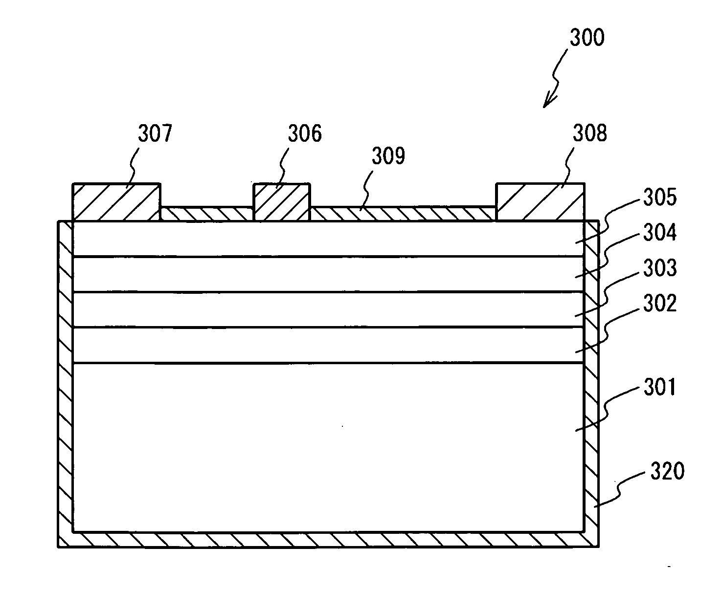
[0062]FIG. 7 is a typical cross section of a semiconductor device 300 according to a third embodiment (GaN-based HEMT). As shown in FIG. 7, in the semiconductor device 300, a buffer layer 302, a channel layer 303, an electron supply layer 304, and a cap layer 305 are sequentially formed over a substrate 301. For example, the substrate 301 is made of SiC, th...
PUM
| Property | Measurement | Unit |
|---|---|---|
| thickness | aaaaa | aaaaa |
| semiconductor | aaaaa | aaaaa |
| stress | aaaaa | aaaaa |
Abstract
Description
Claims
Application Information