Method of manufacturing flexible circuit substrate

a flexible circuit and substrate technology, applied in the direction of circuit inspection/indentification, semiconductor/solid-state device details, instruments, etc., can solve problems such as difficult to occur, and achieve the effect of finer pitch and easy handling

Inactive Publication Date: 2006-10-05
SHINKO ELECTRIC IND CO LTD
View PDF0 Cites 33 Cited by
  • Summary
  • Abstract
  • Description
  • Claims
  • Application Information

AI Technical Summary

Benefits of technology

[0018] The present invention has been made in view of the above circumstances, and it is an object of the present invention to provide a method of manufacturing a flexible circuit substrate, capable of responding easily to a finer pitch between wiring layers and an increase of the number of multiple wiring layers.
[0023] There is no chance that the connection pads, the alignment marks, and the insulating layers connected to the metal thin plate are displaced due to the expansion and the contraction. Therefore, an alignment precision of the connection pads, the via holes, and the like can be improved remarkably rather than the case where the polyimide tape is employed.
[0024] Then, the metal thin plate as the temporal supporting substrate is removed, and thus the flexible circuit substrate employing the insulating layer as the flexible substrate can be obtained.
[0025] In this manner, in the present invention, the built-up wiring layer is formed with good positional precision by utilizing the alignment mark formed on the metal thin plate as the temporal supporting substrate, and then the flexible circuit substrate is obtained by removing the metal thin plate. Therefore, the present invention can deal easily with a finer pitch between the connection pads and the wiring layers and an increase of the number of multiple wiring layers.
[0032] As described above, the method of manufacturing the flexible circuit substrate of the present invention can deal easily with a finer pitch between the wiring layers and an increase of the number of multiple wiring layers.

Problems solved by technology

Unlike the case where the thin polyimide tape is processed by the reel-to-reel transfer, the metal thin plate is never expanded and contracted during the manufacturing step and also the trouble is hard to occur at the time of transfer since the metal thin plate has both a flexibility and some rigidity.

Method used


Image

  • Method of manufacturing flexible circuit substrate
  • Method of manufacturing flexible circuit substrate
  • Method of manufacturing flexible circuit substrate

Examples


first embodiment

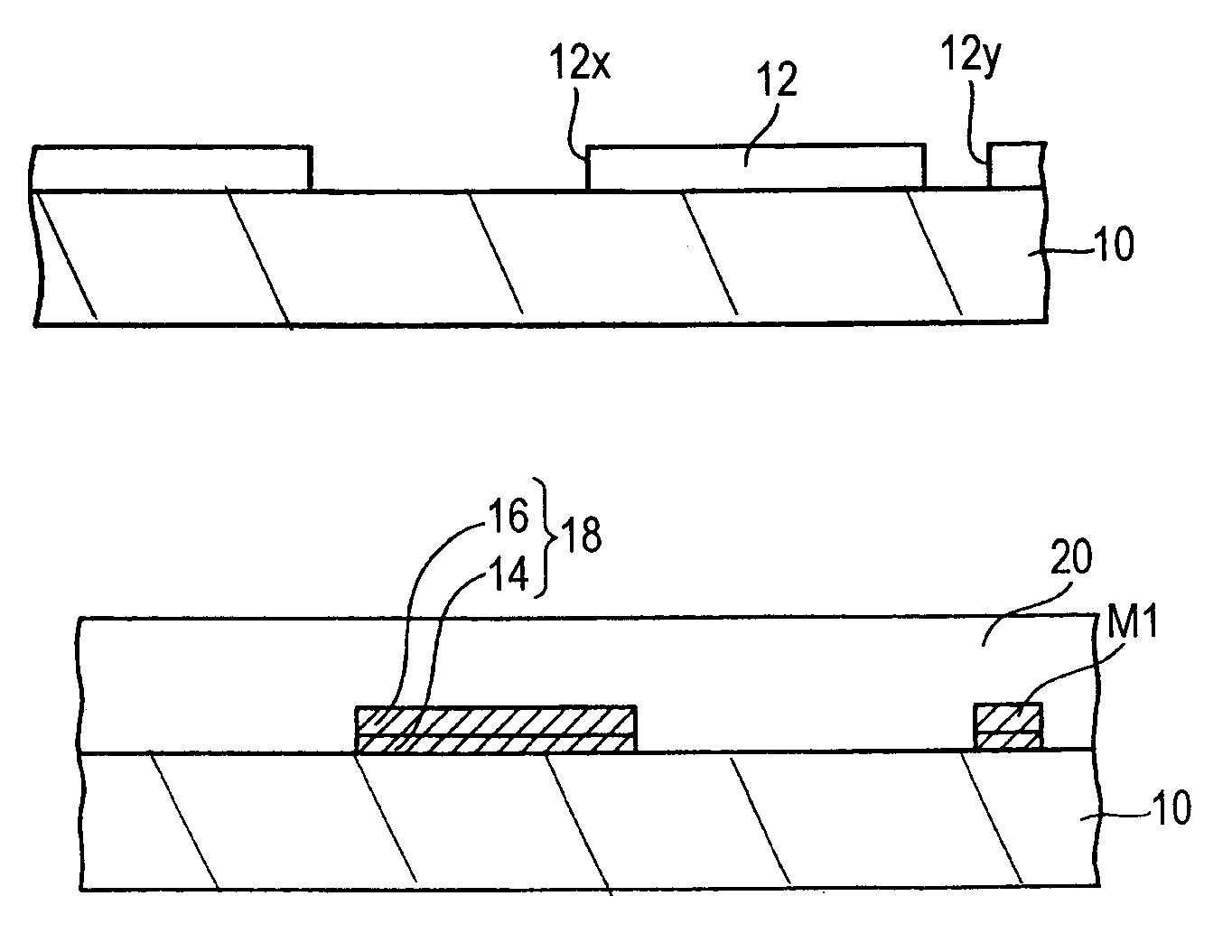
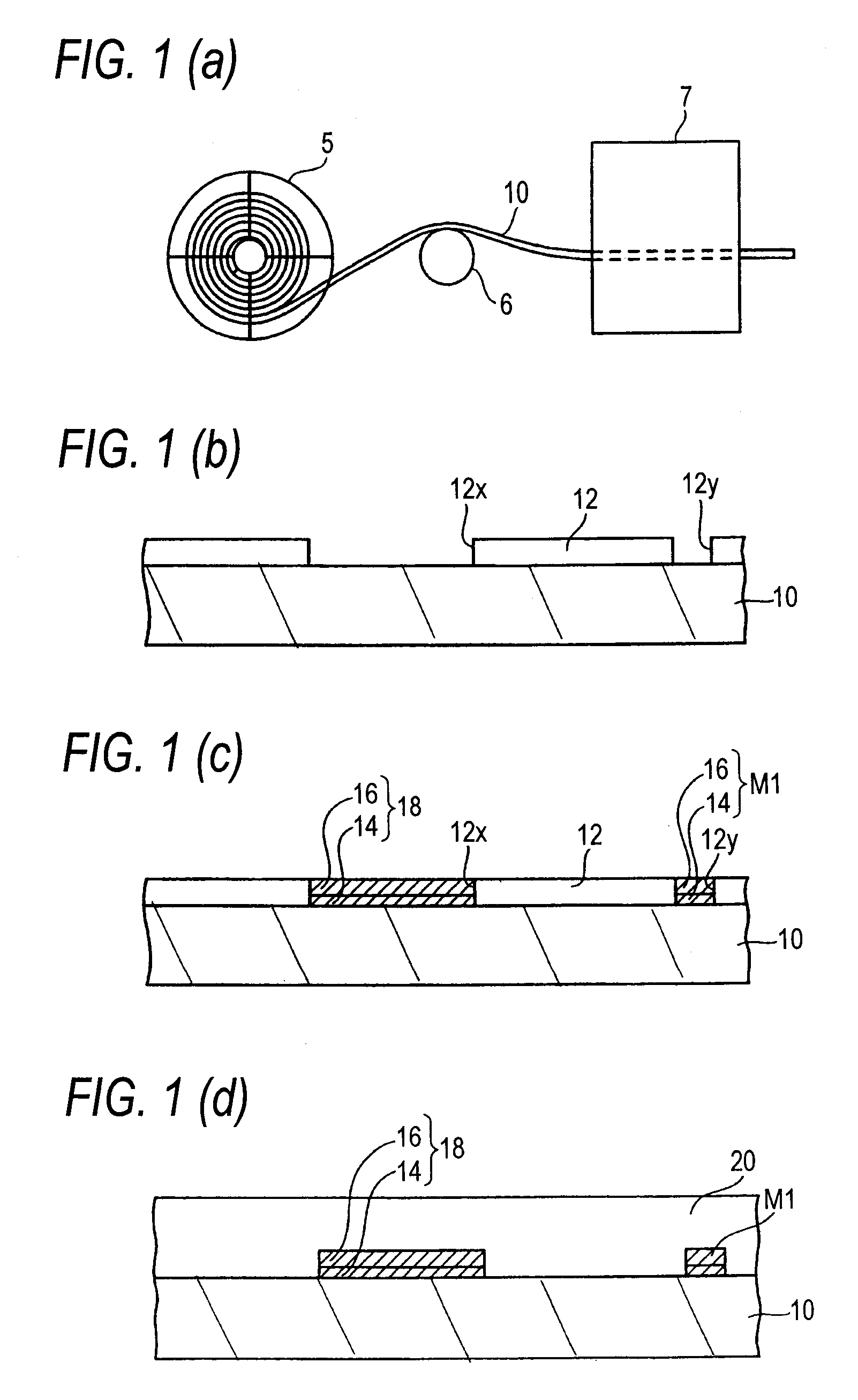
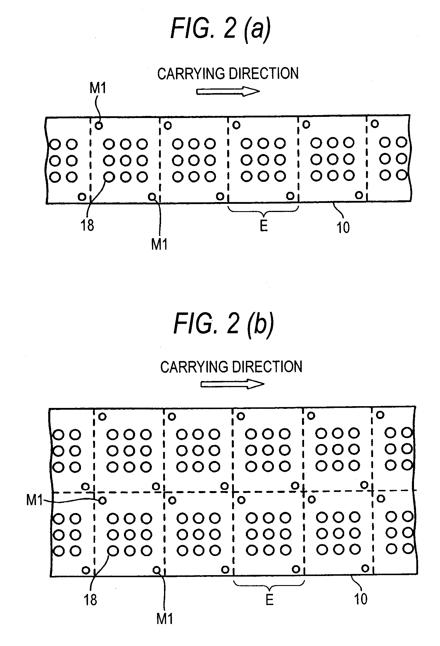
[0050]FIG. 1 to FIG. 6 are sectional views showing a method of manufacturing a flexible circuit substrate according to a first exemplary, non-limiting embodiment of the present invention. In the method of manufacturing the flexible circuit substrate of the first embodiment of the present invention, as shown in FIG. 1(a), first a long metal thin plate 10 that is unwound from a reel (winding member) 5 and carried in the longitudinal direction is prepared. As the metal thin plate 10, various metal materials can be employed, preferably a copper thin plate having a flexibility should be employed and a thickness thereof should be set to about 0.1 to 0.2 mm. Further, the metal thin plate 10 includes metal foil.

[0051] In the present embodiment, the long metal thin plate 10 that is carried by the reel-to-reel system is used as the temporary supporting substrate. The metal thin plate 10 is unwound from the reel 5 and carried into various manufacturing machines 7 while applying a tension (str...

second embodiment

[0074]FIG. 8 to FIG. 10 are sectional views showing a method of manufacturing a flexible circuit substrate according to a second exemplary, non-limiting embodiment of the present invention. A difference of the second embodiment from the first embodiment resides in that a concave portion is provided to the portion of the metal thin plate on which the connection pad is arranged and then a projected portion (external connection terminal) connected to the connection pad is formed simultaneously in forming the connection pad. In the second embodiment, detailed explanations of the same steps as those in the first embodiment will be omitted herein.

[0075] In the method of manufacturing the flexible circuit substrate of the second embodiment, like the first embodiment, as shown in FIG. 8(a), first the resist film 12 in which the first and second opening portions 12x, 12y are provided is formed on the metal thin plate 10. Then, as shown in FIG. 8(b), a first concave portion 10a used to form ...

third embodiment

[0085]FIG. 11 to FIG. 13 are sectional views showing a method of manufacturing a flexible circuit substrate according to a third exemplary, non-limiting embodiment of the present invention. A difference of the third embodiment from the second embodiment is that the metal layers are not filled in the concave portions in the metal thin plate but formed like a layer and then the resin is filled in remaining spaces of the concave portions. In the third embodiment, detailed explanation of the same steps as those in the first and second embodiments will be omitted herein.

[0086] First, as shown in FIG. 11(a), the resist film 12 in which the first and second opening portions 12x, 12y are provided is patterned, as in FIG. 8(b), by the similar method to the second embodiment. Then, the first and second concave portions 10a, 10b are formed in the metal thin plate 10. Then, the barrier contact layer 14 and the Cu plating layer 16 are formed sequentially in the first and second concave portions...


PUM


Abstract

Connection pads and alignment marks are formed on a long metal thin plate that is carried in a longitudinal direction, and then an insulating layer for covering the connection pads is formed. Then, via holes, which are aligned and arranged on the connection pads by utilizing the alignment marks, are formed in portions of the insulating layer. Then, n-layered (n is an integer of 1 or more) wiring layers connected to the connection pads via the via holes are formed, and the connection pads and the insulating layer are exposed by removing the metal thin plate.

Description

[0001] The present application claims foreign priority based on Japanese Patent Application No. 2005-098938, filed Mar. 30, 2005, the content of which is incorporated herein by reference. BACKGROUND OF THE INVENTION [0002] 1. Technical Field [0003] The present invention relates to a method of manufacturing a flexible circuit substrate and, more particularly, a method of manufacturing a flexible circuit substrate, which is applicable in a tape package such as a tape BGA, a tape CSP, or the like. [0004] 2. Related Art [0005] In the related art, there are the tape packages such as the tape BGA (Ball Grid Array), the tape CSP (Chip Size Package), and the like using the polyimide tape as the substrate. In an example of the method of manufacturing the tape package in the related art, as shown in FIG. 14(a), first a polyimide tape 100 on both sides of which copper (Cu) layers 102a, 102b are provided is prepared. This polyimide tape 100 is pulled out from the reel, then carried by the so-ca...

Claims


Application Information

Patent Timeline
Patent Type & Authority Applications(United States)
IPC IPC(8): H01L21/00
CPCH05K2201/096H05K2201/09918H01L2924/15311H01L2224/73265H01L2224/48228H01L2224/48227H01L2224/48091H01L2224/32225H01L2224/16227H01L2224/16225H01L24/48H05K2201/09481H05K2201/0367H05K3/4682H05K3/4679H05K3/4635H05K3/4007H05K3/205H05K3/0035H05K3/0023H05K3/0008H01L23/49827H01L23/4985H05K1/0269H05K1/0393H01L2924/00014H01L2924/00H01L2924/00012H01L24/73H01L2924/181H01L2224/45099H01L2224/45015H01L2924/207G07D2211/00
Inventor NOMURA, TOMOHIROABE, KAZUNORI
Owner SHINKO ELECTRIC IND CO LTD
Why Eureka
Try Eureka