Direct ion beam deposition method and system

a technology of direct ion beam and deposition method, which is applied in the direction of vacuum evaporation coating, electrolysis components, coatings, etc., can solve the problems of uniform electromagnetic, rf process has a limitation in manufacturing high-quality thin films, and rf process has a limitation in uniformity, so as to facilitate ion emission of the deposit material and prevent overheating of the deposit material

Inactive Publication Date: 2006-10-12
SONG SEOK KYUN
View PDF5 Cites 16 Cited by
  • Summary
  • Abstract
  • Description
  • Claims
  • Application Information

AI Technical Summary

Benefits of technology

[0033] According to another aspect of the invention, there is provided with a direct ion beam deposition system using ion beam sputtering. The system includes: an electron emitter means for emitting initial electrons for ion beam generation within a certain operating pressure; an electron guide means for supplying a working gas for formation of plasma atmosphere and guiding into the working gas the electron flow generated from the electron emitter means; an upper case for fixing the position of the electron guide means; an electromagnetic field formation means placed in the outer periphery of the upper case for forming a certain magnitude of electromagnetic field such that electrons emitted from the electron emitter means is turned when guided by the electron gui

Problems solved by technology

First, the RF process has a limitation in its uniformity due to the non-uniform electromagnetic field, instability and inefficiency due to the matching to the expensive power supply equipment, interference with peripheral devices, and the high operating pressure of 10−3 to 10−2 torr.
Thus, the RF process has a limitation in manufacturing a high quality thin film.
In addition, the microwave process has a limitation in the large-area and inconvenient maintenance due to the high priced power supply and the service life of about 6,000 hours, and thus its application is very

Method used


Image

  • Direct ion beam deposition method and system
  • Direct ion beam deposition method and system
  • Direct ion beam deposition method and system

Examples


Embodiment Construction

[0059] The preferred embodiments of the invention will be hereafter described in detail, with reference to the accompanying drawings.

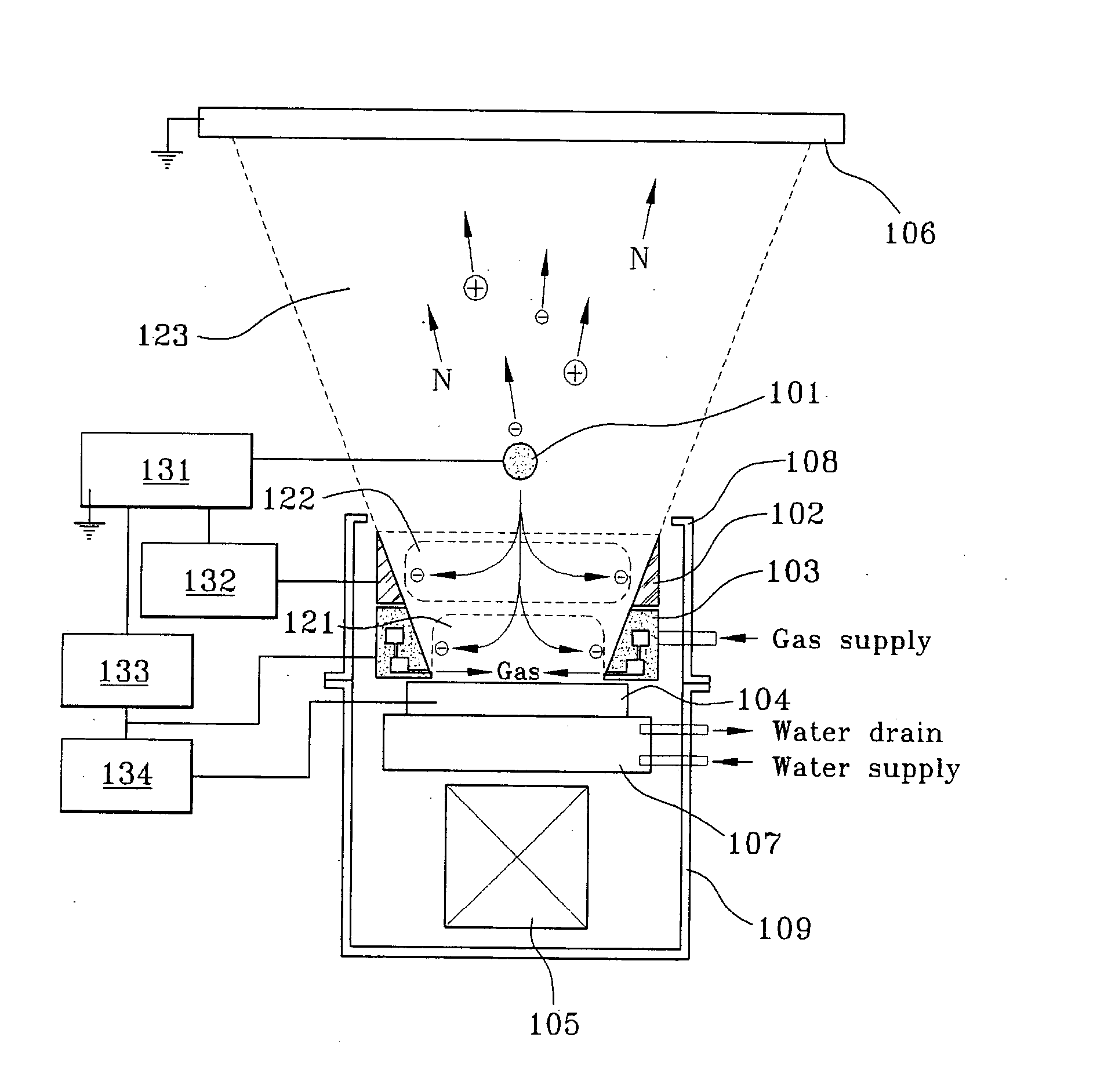
[0060]FIG. 4 is a schematic view of a direct ion beam deposition system through ion beam sputtering according to the invention. FIG. 5 is a perspective view of part of the system in FIG. 4. FIG. 6 shows the structure of an anode in the direct ion beam deposition system of the invention. FIG. 7 is a sectional and perspective view of the structure of a first anode in FIGS. 4 to 6, where the first anode is indicated by reference numeral 103.

[0061] Referring to FIGS. 4 to 7, the construction and operation of a direct ion beam deposition system through ion beam sputtering according to the invention will be described.

[0062] As illustrated in FIGS. 4 and 5, the direct ion beam deposition system through ion beam sputtering according to the invention includes a filament cathode 101 for generating initial charges to generate ion beam, an anode 102, 103 for gu...


PUM

PropertyMeasurementUnit
Pressureaaaaaaaaaa
Pressureaaaaaaaaaa
Lengthaaaaaaaaaa

Abstract

Disclosed herein is a direct ion beam deposition method through ion beam sputtering. The method comprises the steps of: a) providing a workpiece on which a certain material is to be deposited with a certain desired thickness; b) providing a deposit material having a certain area from which the deposit material is discharged into a certain working gas atmosphere; c) transforming the working gas atmosphere into a plasma atmosphere by bombarding electrons widely to the working gas atmosphere; d) emitting a surface material by means of a sputter from the deposit material exposed in the plasma atmosphere; e) exposing the emitted deposit material to an ionization environment; f) and providing energy to the deposit material by applying an electric potential to the step e) to thereby be radiated on a corresponding face of the workpiece. A direct ion beam deposition system is also disclosed.

Description

[0001] The application claims and requests a foreign priority, through the Paris Convention for protection of Industrial Property, based on a patent application filed in the Republic of Korea with number 10-2005-0030228, by the applicant, the contents of which are incorporated by reference into this disclosure as if fully set forth herein. BACKGROUND OF THE INVENTION [0002] 1. Field of the Invention [0003] The present invention relates to a direct ion beam deposition system. In particular, the invention relates to a direct ion beam deposition method and system through ion beam sputtering, in which a direct ion beam deposition mode and an ion beam sputtering deposition mode are combined to thereby enable a thin film deposition over a large-area under a low pressure by the direct ion beam deposition mode and simultaneously to enable a high quality thin film deposition. [0004] 2. Background of the Related Art [0005] In general, the semiconductor processing techniques are fundamental to...

Claims


Application Information

Patent Timeline
IPC IPC(8): C23C14/00C23C14/35C23C14/46H01J37/32
CPCC23C14/355H01J37/32724H01J37/3233H01J37/32009C23C14/46C23C14/221C23C14/3442C23C14/14H01L21/02631
Inventor SONG, SEOK KYUN
Owner SONG SEOK KYUN
Why Eureka
Try Eureka