Etching method

a technology of etching and etching rate, which is applied in the direction of decorative surface effects, electrical appliances, decorative arts, etc., can solve the problems of degassing, delay in wiring time, and obstacle to the implementation of a semiconductor integrated circuit with higher performance, so as to improve the anisotropic property of etching and the etching rate.

Inactive Publication Date: 2006-10-12
PANASONIC CORP
View PDF9 Cites 210 Cited by
  • Summary
  • Abstract
  • Description
  • Claims
  • Application Information

AI Technical Summary

Benefits of technology

[0069] Thus, the twelfth etching method allows highly anisotropic etching to be performed with respect to the organic-inorganic hybrid film without incurring the degradation thereof.
[0070]

Problems solved by technology

As the integration density of a semiconductor integrated circuit has increased, an increased wiring delay time resulting from an increase in wire-to-wire capacitance, which is a parasitic capacitance between metal wires, has presented an obstacle to the implementation of a semiconductor integrated circuit with higher performance.
However, since the organic compound film and the organic-inorganic hybrid film are highly susceptible to oxidization, the problem is encountered that degassing occurs in a heat treatment process subsequently performed.
During etching, however, the quality of the organic compound film is degraded by oxygen because of high reactivity of the organic compound film to oxygen.
When the gas is generated

Method used


Image

  • Etching method

Examples


embodiment 1

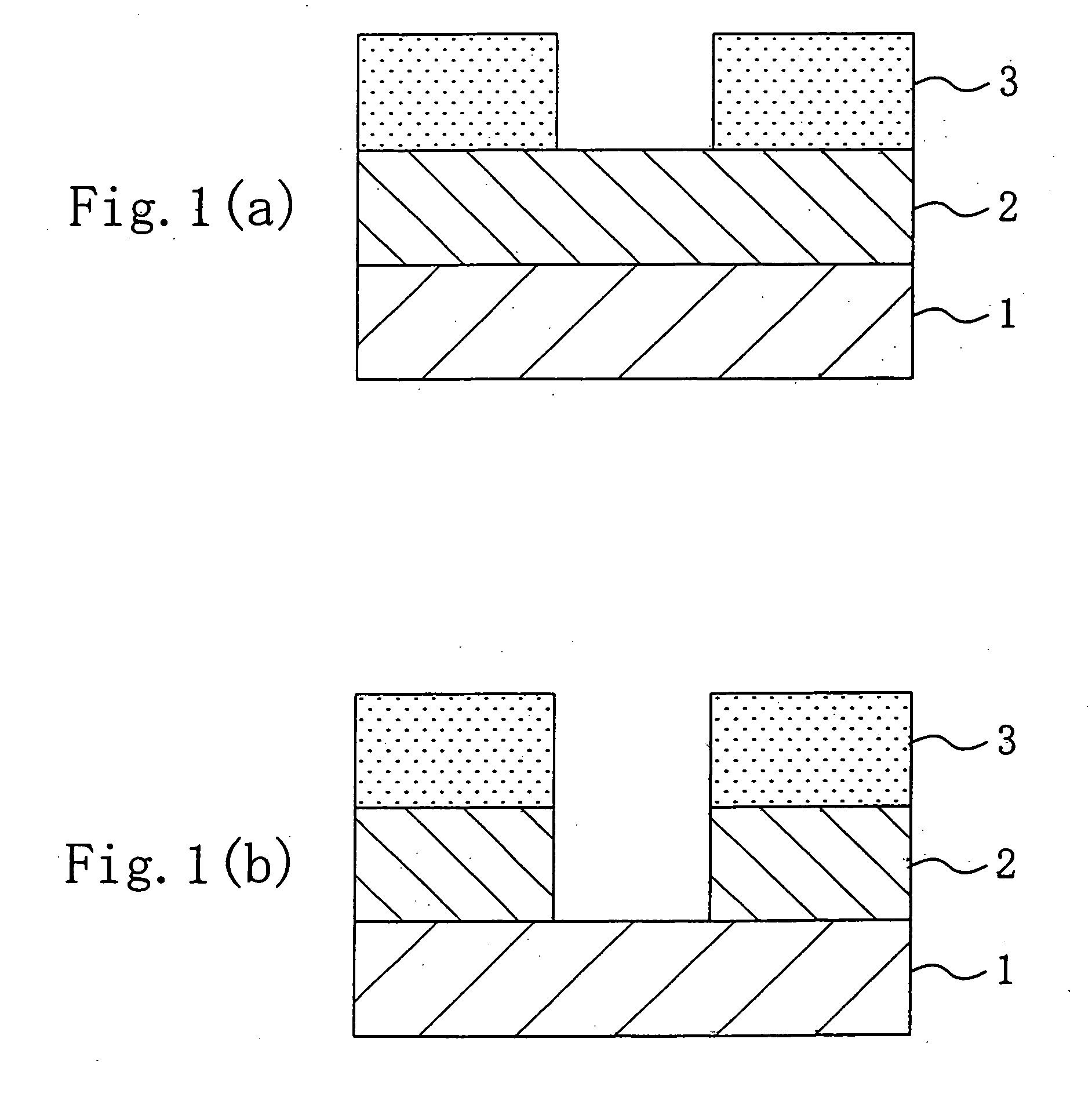
[0075] A first embodiment of the present invention performs anisotropic etching with respect to an interlayer insulating film composed of an organic compound film by using a plasma derived from an etching gas containing ammonia gas as a main constituent.

[0076] As an exemplary organic compound film, there can be listed a derivative of polyaryl ether or a derivative of polyparaxylene. However, the type of the organic compound film does not particularly presents a problem.

[0077] By way of example, etching is performed in an etching apparatus using a high-density plasma as a plasma source under such conditions that pressure is 5 mTorr, the power of an RF voltage applied to a counter electrode is 3 kW, the power of a bias voltage applied to a sample to be etched is 300 W, and the flow rate of ammonia (NH3) gas is 20 sccm.

[0078] When etching is performed with respect to the organic compound film by using the plasma derived from the etching gas containing ammonia gas as the main constit...

embodiment 2

[0081] A second embodiment of the present invention performs anisotropic etching with respect to an interlayer insulating film composed of an organic compound film by using a plasma derived from an etching gas containing hydrogen gas, nitrogen gas, and inert gas (such as argon gas) as main constituents.

[0082] As an exemplary organic compound film, there can be listed a derivative of polyaryl ether or a derivative of polyparaxylene. However, the type of the organic compound film does not particularly present a problem.

[0083] By way of example, etching is performed in an etching apparatus using a high-density plasma as a plasma source under such conditions that pressure is 10 mTorr, the power of an RF voltage applied to a counter electrode is 3 kW, the power of a bias voltage applied to a sample to be etched is 200 W, the flow rate of hydrogen gas is 30 sccm, the flow rate of nitrogen gas is 10 sccm, and the flow rate of argon gas is 20 sccm.

[0084] When etching is performed with re...

embodiment 3

[0091] A third embodiment of the present invention performs anisotropic etching with respect to an interlayer insulating film composed of an organic compound film by using a plasma derived from an etching gas containing ammonia gas and inert gas (such as argon gas) as main constituents.

[0092] As an exemplary organic compound film, there can be listed a derivative of polyaryl ether or a derivative of polyparaxylene. However, the type of the organic compound film does not particularly present a problem.

[0093] By way of example, etching is performed in an etching apparatus using a high-density plasma as a plasma source under such conditions that pressure is 30 mTorr, the power of an RF voltage applied to a counter electrode is 3 kW, the power of a bias voltage applied to a sample to be etched is 200 W, the flow rate of ammonia gas is 30 sccm, and the flow rate of argon gas is 20 sccm.

[0094] When etching is performed with respect to the organic compound film by using the plasma deriv...


PUM

PropertyMeasurementUnit
Anisotropyaaaaaaaaaa
aaaaaaaaaa

Abstract

An interlayer insulating film composed of an organic compound film containing an organic component as a main constituent is deposited on a semiconductor substrate. Then, etching is performed with respect to the interlayer insulating film by using a plasma derived from an etching gas containing an ammonia gas as a main constituent. As a result, active hydrogen is generated in the plasma derived from the ammonia gas to decompose the organic component into hydrogen cyanide, whereby etching proceeds. Since a surface of the organic compound film is efficiently nitrided by nitrogen generated from the ammonia gas, the sidewalls of a depressed portion in the organic compound film are protected so that an excellent anisotropic property is provided. Since the etching gas does not contain a component which oxidizes the organic compound film, the problem does not occur that a gas is generated from the organic compound film in a subsequent heat treatment process.

Description

BACKGROUND OF THE INVENTION [0001] The present invention relates to an etching method and, more particularly to anisotropic etching performed with respect to an interlayer insulating film composed of an organic compound film containing an organic component as a main constituent or to an interlayer insulating film composed of an organic-inorganic hybrid film containing an organic component and a silica component as main constituents.[0002] As the integration density of a semiconductor integrated circuit has increased, an increased wiring delay time resulting from an increase in wire-to-wire capacitance, which is a parasitic capacitance between metal wires, has presented an obstacle to the implementation of a semiconductor integrated circuit with higher performance. The wiring delay time is a so-called RC delay which is proportional to the product of the resistance of the metal wire and the wire-to-wire capacitance. [0003] To reduce the wiring delay time, therefore, it is necessary to...

Claims


Application Information

Patent Timeline
IPC IPC(8): C23F1/00H01L21/302H01L21/3065H01L21/311
CPCH01L21/31138H01L21/31116
Inventor AOI, NOBUO
Owner PANASONIC CORP
Why Eureka
Try Eureka