Light emitting device and fabricating method thereof

a technology of light emitting device and fabrication method, which is applied in the direction of discharge tube/lamp details, discharge tube luminescent screen, discharge tube/lamp details, etc., can solve the problems of poor color reproducibility, no suggestion about an optimal combination, and inability to obtain a semiconductor light source having good luminous efficiency, etc., to achieve high luminance, easy color setting, and high efficiency

Active Publication Date: 2006-10-12
SHARP KK
View PDF20 Cites 187 Cited by
  • Summary
  • Abstract
  • Description
  • Claims
  • Application Information

AI Technical Summary

Benefits of technology

[0021] In view of the above-described state of the prior art, an object of the present invention is to provide a light-emitting device that includes a wavelength conversion unit containing plural kinds of phosphors for emitting light with high efficiency in response to light in the wavelength range from 380 n...

Problems solved by technology

However, it is not possible to obtain a semiconductor light source having good luminous efficiency of green.
Further, the luminance of each of the semiconductor light sources needs to be controlled independently from each other, which requires a drive circuit of a large scale.
With this method, however, there is a problem that the color reproducibility is poor, since the spectral purity of green is low, in addition to insufficient red component.
The document however gives no suggestion about an optimal combination of the LED and the plural kinds of phosphors, particula...

Method used


Image

  • Light emitting device and fabricating method thereof
  • Light emitting device and fabricating method thereof
  • Light emitting device and fabricating method thereof

Examples


example 1

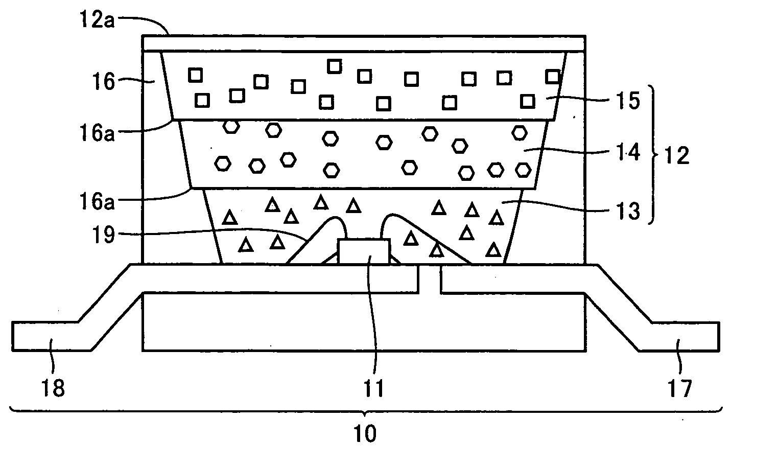
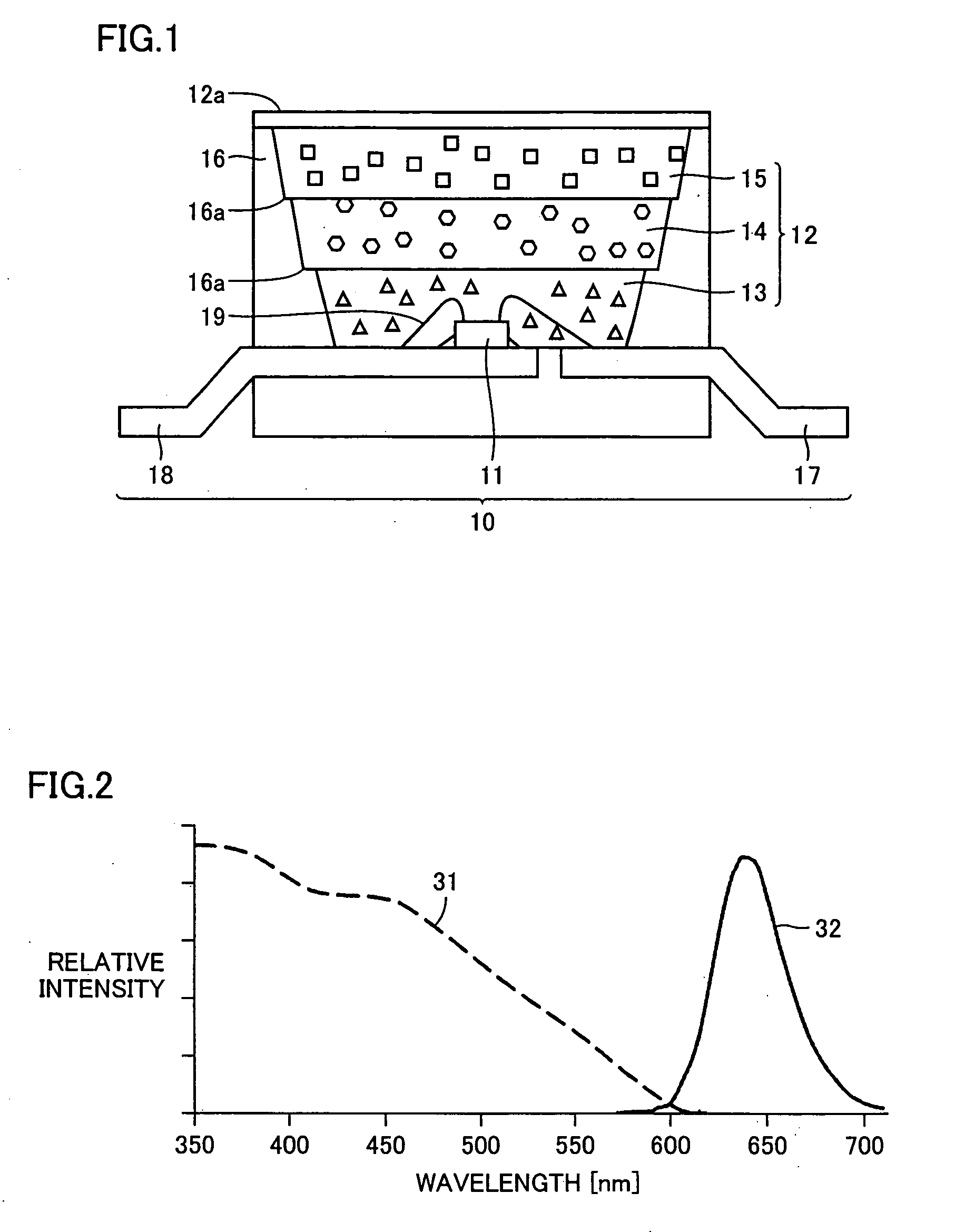
[0049] In FIG. 1, a light-emitting device according to Example 1 of the present invention is illustrated in a schematic vertical cross sectional view. This light-emitting device 10 includes a light-emitting element 11 for emitting primary light, and a wavelength conversion unit 12 that absorbs at least part of the primary light and emits secondary light having a wavelength longer than that of the primary light. Light-emitting element 11 is mounted on a cathode terminal 18 and it is electrically connected to an anode terminal 17 and cathode terminal 18 via gold wires 19.

[0050] For light-emitting element 11, it is possible to use a gallium nitride (GaN)-based light-emitting diode having an emission peak wavelength at 410 nm, for example.

[0051] Wavelength conversion unit 12 includes a layer 13 that contains a phosphor having a composition of (Ca0.98Eu0.02)AlSiN3 for emitting red light, a layer 14 that contains a phosphor having a composition of (Ba0.85Eu0.15) (Mg0.80Mn0.20)Al10O17 fo...

example 2

[0064] In Example 2 of the present invention, a gallium nitride (GaN)-based light-emitting diode having a peak wavelength at 460 nm was used as the light-emitting element.

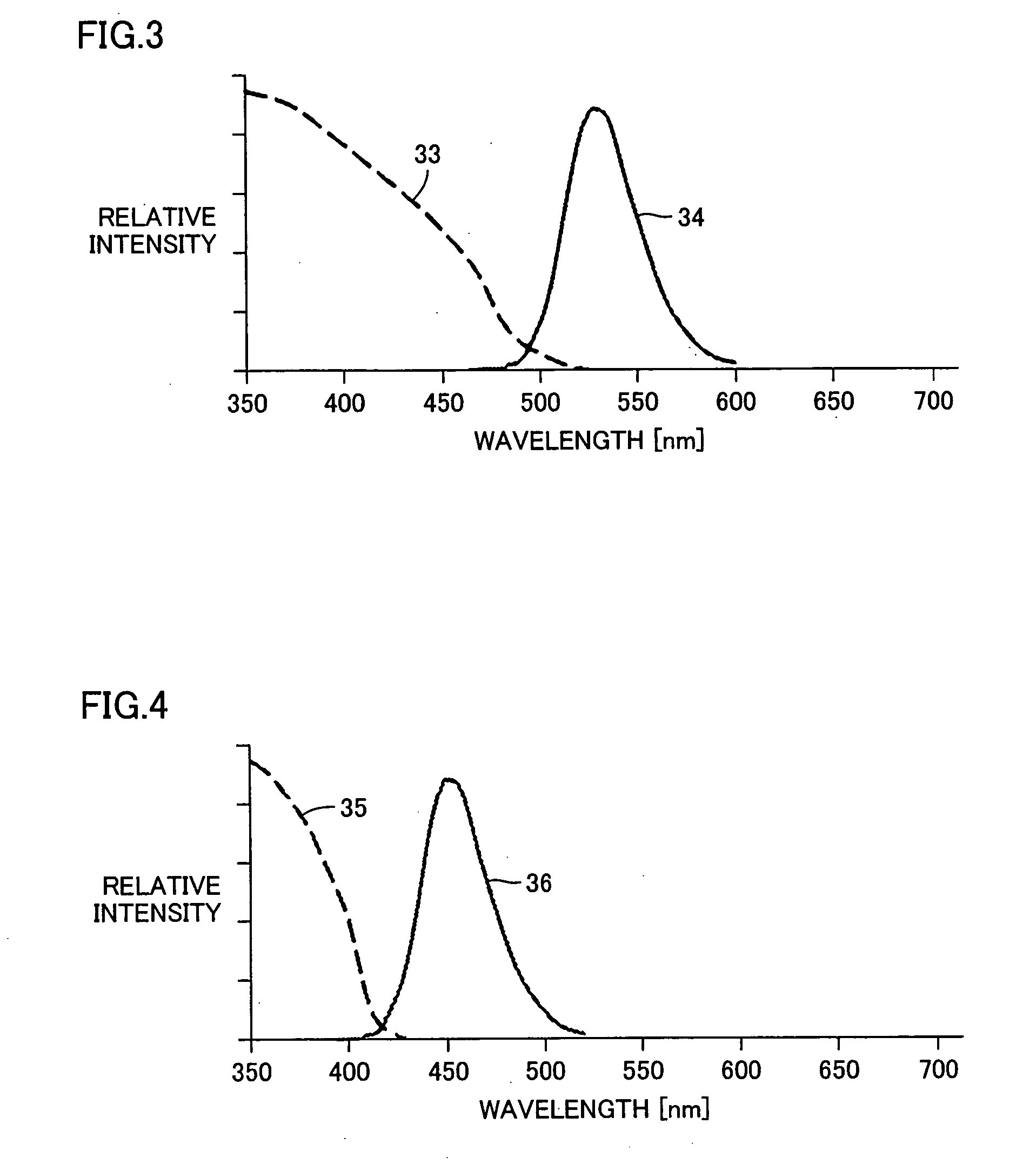
[0065] For the wavelength conversion unit, there were used a phosphor for green light represented by a composition of (Sr0.75Ba0.24Eu0.01)2SiO4 and a phosphor for red light represented by a composition of (Ca0.985Eu0.015)AlSiN3. It is recognized from FIG. 2 that the phosphor for red light can absorb green light (wavelength near 550 nm) emitted from the phosphor for green light and then can emit red light.

[0066] The light-emitting device of Example 2 was fabricated using the light-emitting diode and the phosphors, in a similar manner as in Example 1. As Comparative Example 2, there was fabricated a light-emitting device having a wavelength conversion unit formed of a single light-emitting layer made by mixing exactly the same kinds of phosphors as in Example 2.

[0067] Properties of the light-emitting devices of Ex...

examples 3-8

[0069] Light-emitting devices of Examples 3-8 and Comparative Examples 3-8 were fabricated in a similar manner as in Example 1 and Comparative Example 1, except that the emission peak wavelengths of the light-emitting elements and the kinds of phosphors used were changed. Evaluation results of their properties are shown in Table 3.

TABLE 3Peak wavelengthBrightnessof primary lightPhosphors(relative value)Tc-duvEx. 3410 nmred: (Ca0.94Sr0.05Eu0.01)AlSiN3100%6500 K − 0.003green: (Sr0.70Ba0.28Eu0.02)2SiO4blue: (Sr0.74Ba0.20Ca0.05Eu0.01)10(PO4)6.Cl2Com. Ex. 3″red: (Ca0.94Sr0.05Eu0.01)AlSiN3 73%″green: (Sr0.70Ba0.28Eu0.02)2SiO4blue: (Sr0.74Ba0.20Ca0.05Eu0.01)10(PO4)6.Cl2Ex. 4410 nmred: (Ca0.99Eu0.01)(Al0.90Ga0.10)SiN3100%7500 K + 0.001green: (Ba0.86Eu0.14)Mg0.75Mn0.25)Al10O17blue: (Ba0.86Eu0.14)(Mg0.99Mn0.01)Al10O17Com. Ex. 4″red: (Ca0.99Eu0.01)(Al0.90Ga0.10)SiN3 70%″green: (Sr0.70Ba0.28Eu0.02)2SiO4blue: (Sr0.74Ba0.20Ca0.05Eu0.01)10(PO4)6.Cl2Ex. 5450 nmred: (Ca0.98Eu0.02)AlSiN3100%5800 K ...


PUM


Abstract

A light-emitting device includes a light-emitting element for emitting primary light, and a wavelength conversion unit for absorbing part of the primary light and emitting secondary light having a wavelength longer than that of the primary light, wherein the wavelength conversion unit includes plural kinds of phosphors having light absorption characteristics different from each other, and then at least one kind of phosphor among the plural kinds of phosphors has an absorption characteristic that can absorb the secondary light emitted from at least another kind of phosphor among the plural kinds of phosphors.

Description

[0001] This nonprovisional application is based on Japanese Patent Applications Nos. 2005-157056, 2005-202851 and 2006-059689 filed with the Japan Patent Office on May 30, 2005, Jul. 12, 2005 and Mar. 6, 2006, respectively, the entire contents of which are hereby incorporated by reference. BACKGROUND OF THE INVENTION [0002] 1. Field of the Invention [0003] The present invention relates to improvement in a light-emitting device or a white light-emitting device including a semiconductor light-emitting element for emitting primary light and a wavelength conversion unit containing phosphor for absorbing the primary light and then emitting secondary light. [0004] 2. Description of the Background Art [0005] The light-emitting device or the white light-emitting device including the semiconductor light-emitting element and the wavelength conversion unit has attracted attention as a light-emitting device or a white light-emitting device of next generation expected to realize low power consum...

Claims


Application Information

Patent Timeline
IPC IPC(8): H01J1/62H01L33/32H01L33/50H01L33/54H01L33/56H01L33/62
CPCC09K11/0883C09K11/7721H01L2224/45144H01L2224/73265H01L2224/48247H01L2224/48091H01L2224/32245H01L2933/0041H01L33/504C09K11/7728C09K11/7734C09K11/7739C09K11/7774H01J1/63H01L2924/00014H01L2924/00C09K11/77214C09K11/77342C09K11/77348H01L33/508H01L33/505
Inventor MASUDA, MASATSUGUKATOH, MASAAKIINOGUCHI, TSUKASA
Owner SHARP KK
Why Eureka
Try Eureka