Semiconductor laser device and heat sink used therein

Inactive Publication Date: 2006-10-12
SONY CORP
View PDF7 Cites 36 Cited by
  • Summary
  • Abstract
  • Description
  • Claims
  • Application Information

AI Technical Summary

Benefits of technology

[0016] According to any embodiments of the invention, heat generated when driving the semiconductor laser element is transferred to the heat sink. The heat sink having a channel in which a coolant, for example, water, flows inside thereof removes the heat received from the semiconductor laser element. This allows the semiconductor laser element to be cooled.
[0017] In the heat sink, the mounting plate portion on which the semiconductor laser element is mounted is made of material having a thermal expansion coefficient, which is nearer that of the semiconductor laser element than that of the channel-forming plate portion. This allows any stress generated in the semiconductor laser element to be reduced when expanding and contracting the semiconductor laser element and the mounting plate portion based on the heat generated for driving th

Problems solved by technology

If the indium solder is used for bonding the semiconductor laser chip, the solder may show fragility due to alloyed indium solder when turning on electricity through the semiconductor laser chip for a long time and hence, reliability of the chip deteriorates.
However, corrosion of the metal material may occur at this portion, thereby causing wate

Method used


Image

  • Semiconductor laser device and heat sink used therein
  • Semiconductor laser device and heat sink used therein
  • Semiconductor laser device and heat sink used therein

Examples


first embodiment

[0027] (A Configuration of First Embodiment of Semiconductor Laser Device According to the Invention)

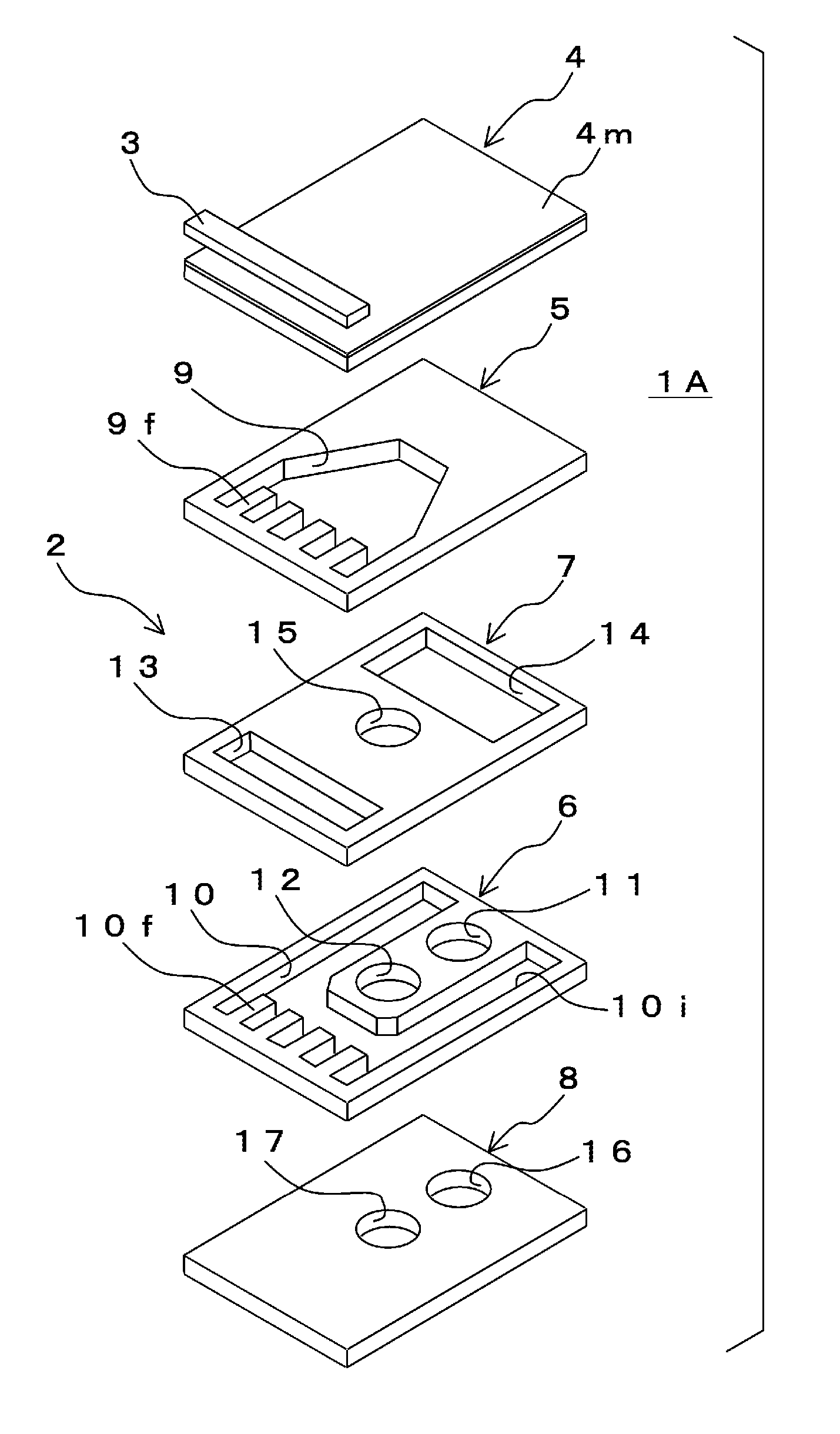
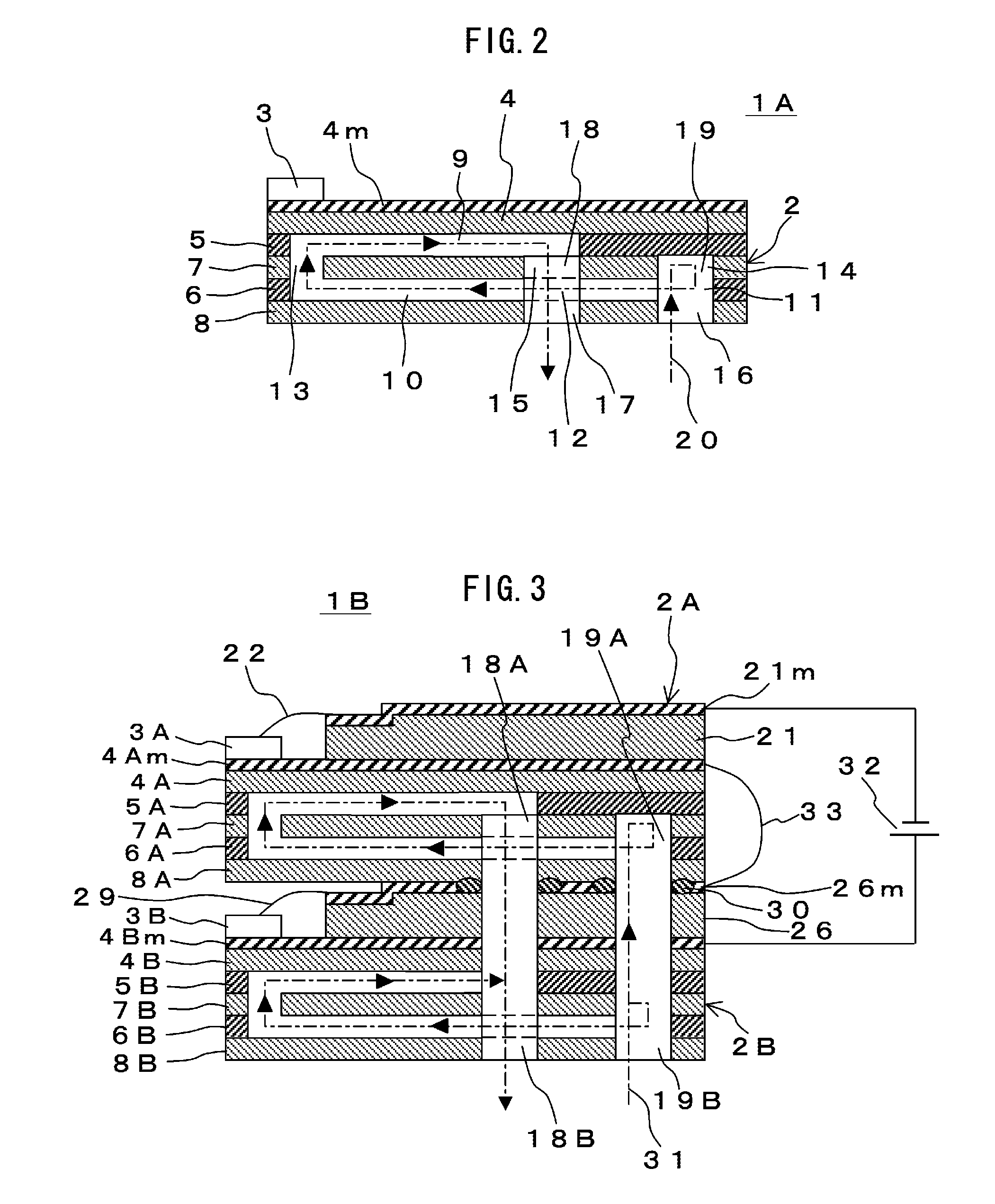
[0028]FIG. 1 is an exploded perspective view of a first embodiment of each of the semiconductor laser device and the heat sink used therein according to the invention for illustrating a configuration thereof. FIG. 2 is a sectional side elevation of the first embodiment of the semiconductor laser device according to the invention for illustrating a configuration thereof.

[0029] A first embodiment of the semiconductor laser device 1A contains a heat sink 2 having a fine channel structure of micro channel type and a semiconductor laser chip 3 mounted thereon. This embodiment of the heat sink 2 is constituted of laminated thin plates. In this embodiment, the heat sink 2 is constituted of the following plates as five layers: a laser-chip-mounting plate 4 as a first layer; radiation-fin-forming plates 5, 6 as second and fourth layers; and channel-forming plates 7, 8 as third and fifth laye...

second embodiment

[0067] (A Configuration of Second Embodiment of Semiconductor Laser Device According to the Invention)

[0068]FIG. 3 is a sectional side elevation of a second embodiment of a semiconductor laser device according to the invention for illustrating a configuration thereof.

[0069] This semiconductor laser device 1B in the second embodiment is a semiconductor laser device of so-called stack type in which, for example, two semiconductor laser devices 1A in the first embodiment are stacked in a vertical direction thereof.

[0070] It is to be noted that although two semiconductor laser devices have been stacked in this embodiment, this invention is not limited to this. For example, twenty semiconductor laser devices can be stacked, thereby implementing any high-power semiconductor laser device.

[0071] Such the semiconductor laser device 1B in this embodiment has an upper heat sink 2A and a lower heat sink 2B each having a fine channel structure of micro channel type. Each of the heat sinks 2A,...


PUM


Abstract

A semiconductor laser device has a heat sink of which laminated plural plates are constituted and a semiconductor laser element mounted on upper surface of the heat sink. The heat sink has a channel in which a coolant flows inside thereof. The heat sink includes a channel-forming plate portion that forms the channel and a mounting plate portion that forms an upper surface of the heat sink that comes into contact with the channel. The mounting plate portion is made of material having a thermal expansion coefficient, which is nearer that of the semiconductor laser element than that of the channel-forming plate portion.

Description

[0001] The present invention contains subject matter related to Japanese Patent Application No. JP2005-115118 filed in the Japanese Patent Office on Apr. 12, 2005, the entire contents of which being incorporated herein by reference. BACKGROUND OF THE INVENTION [0002] 1. Field of the Invention [0003] This invention relates to a semiconductor laser device and a heat sink used therein. [0004] 2. Description of Related Art [0005] A semiconductor laser device in a range from several watts to a few tens watts has often used a water-cooled system therein in order to implement high-power and high-reliability. Heat sink of micro channel type is well known as a heat sink structure to implement high heat-removing efficiency.[0006] As a method of forming a fine interior channel structure such as micro channel typed one, a method of laminating metal thin plates in which a pattern is etched by etching or the like and bonding them by means of diffusion bonding or brazing is generally used. As the ...

Claims


Application Information

Patent Timeline
IPC IPC(8): H01S3/04
CPCH01S5/02272H01S5/02423H01S5/4025H01L2924/0002H01L2924/00H01S5/0237
Inventor KAWANISHI, HIDEKAZUSASAKI, KENJIHAMAGUCHI, YUICHI
Owner SONY CORP
Why Eureka
Try Eureka