

Rear plate for plasma display panel
a plasma display panel and rear plate technology, applied in the manufacture of electrode systems, cold cathode manufacturing, electric discharge tubes/lamps, etc., can solve the problems of deterioration of pdp electrical and optical properties, and achieve the effect of superior electric and optical characteristics
- Summary
- Abstract
- Description
- Claims
- Application Information
AI Technical Summary
Benefits of technology
Problems solved by technology
Method used
Image

Examples
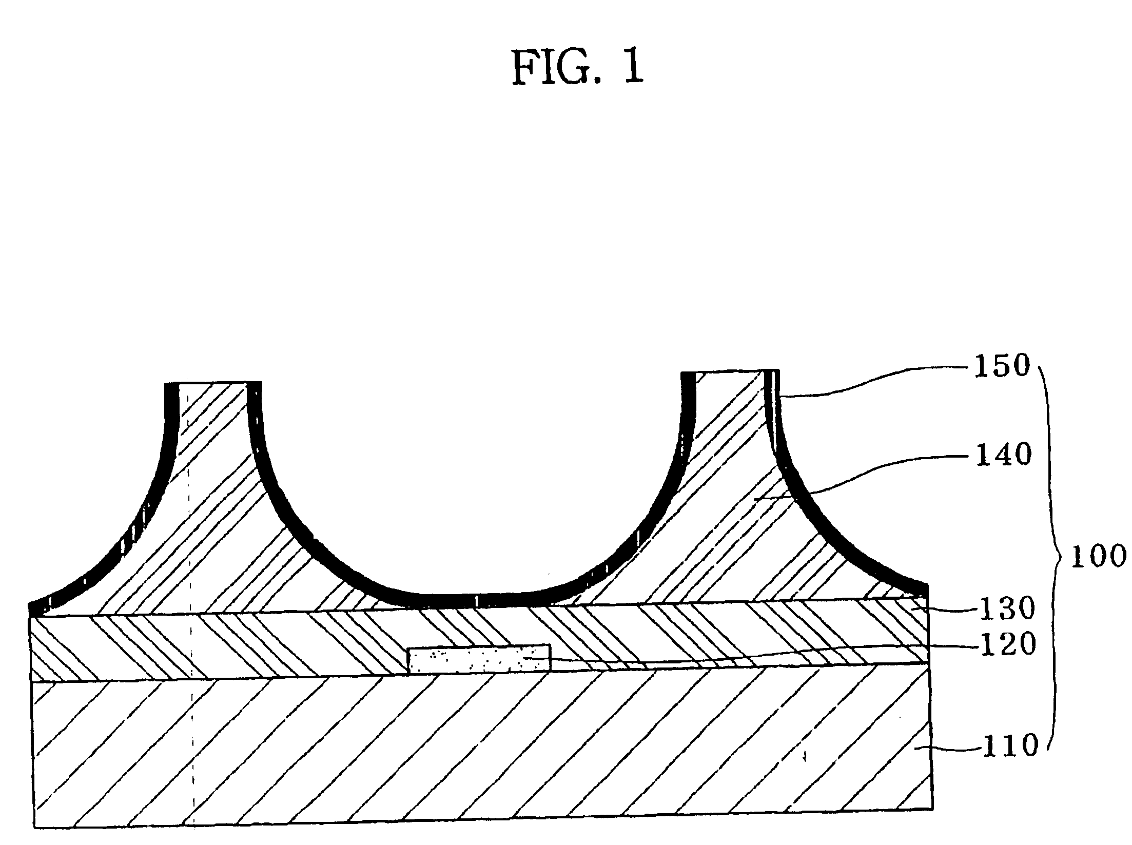
first embodiment
[0022] In the rear plate 100 according to the first embodiment of the present invention, the dielectric layer 130 is formed by a screen printing method, the barrier walls are formed in a shape of green tapes, and then the dielectric layer 130 and the barrier walls are simultaneously baked. This process will be described in detail hereinafter.
[0023] The electrodes 120 formed on the upper surface of the glass substrate has a thickness of 2˜8 μm. That is, photosensitive paste for the electrodes, which has a specific resistance of 2.5×10⁻⁶ to 4.0×10⁻⁶ Ωcm, is screen-printed on the upper surface of the glass substrate 110, is dried, and is then subjected to photolithography and firing, thereby forming the electrodes 120. When the electrodes have a specific resistance of lower than 2.5×10⁻⁶, the low resistance enables the electrodes to process an address signal without noise. However, the electrodes must be made from gold or silver with high purity, which increases the manufacturing cost...
second embodiment
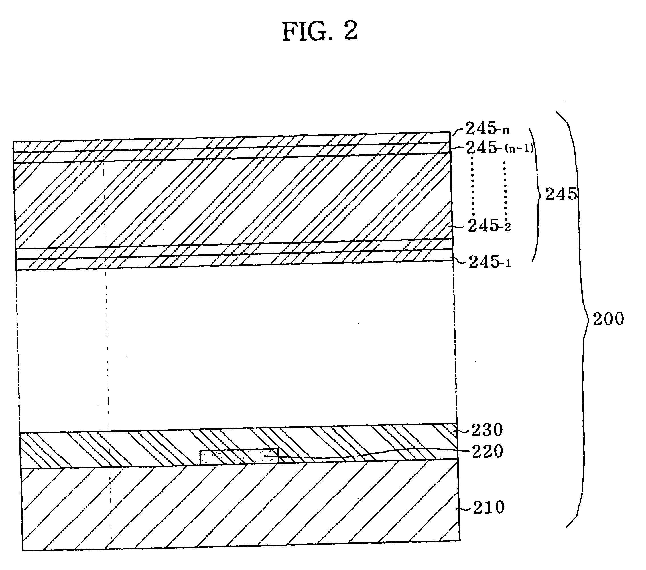
[0054]FIG. 2 is a sectional view of a rear plate of a plasma display panel according to the second embodiment of the present invention.
[0055] As shown, a dielectric layer 230 and barrier walls 245 each are arranged in a shape of green tapes, the dielectric layer 230 is formed on upper surfaces of an electrode 220 and a glass substrate 210, and then the barrier walls 245 are formed on an upper surface of the dielectric layer 230, so that a rear plate 200 according to the second embodiment of the present invention is completed.
[0056] The electrode 220 according to the second embodiment is the same as the electrode according to the first embodiment, and the dielectric layer 230 according to the second embodiment is made from the same material as that of the dielectric layer 130 according to the first embodiment. However, in forming the dielectric layer 230 according to the second embodiment, organic material and additives are added to material of the dielectric layer 130 according to...
third embodiment
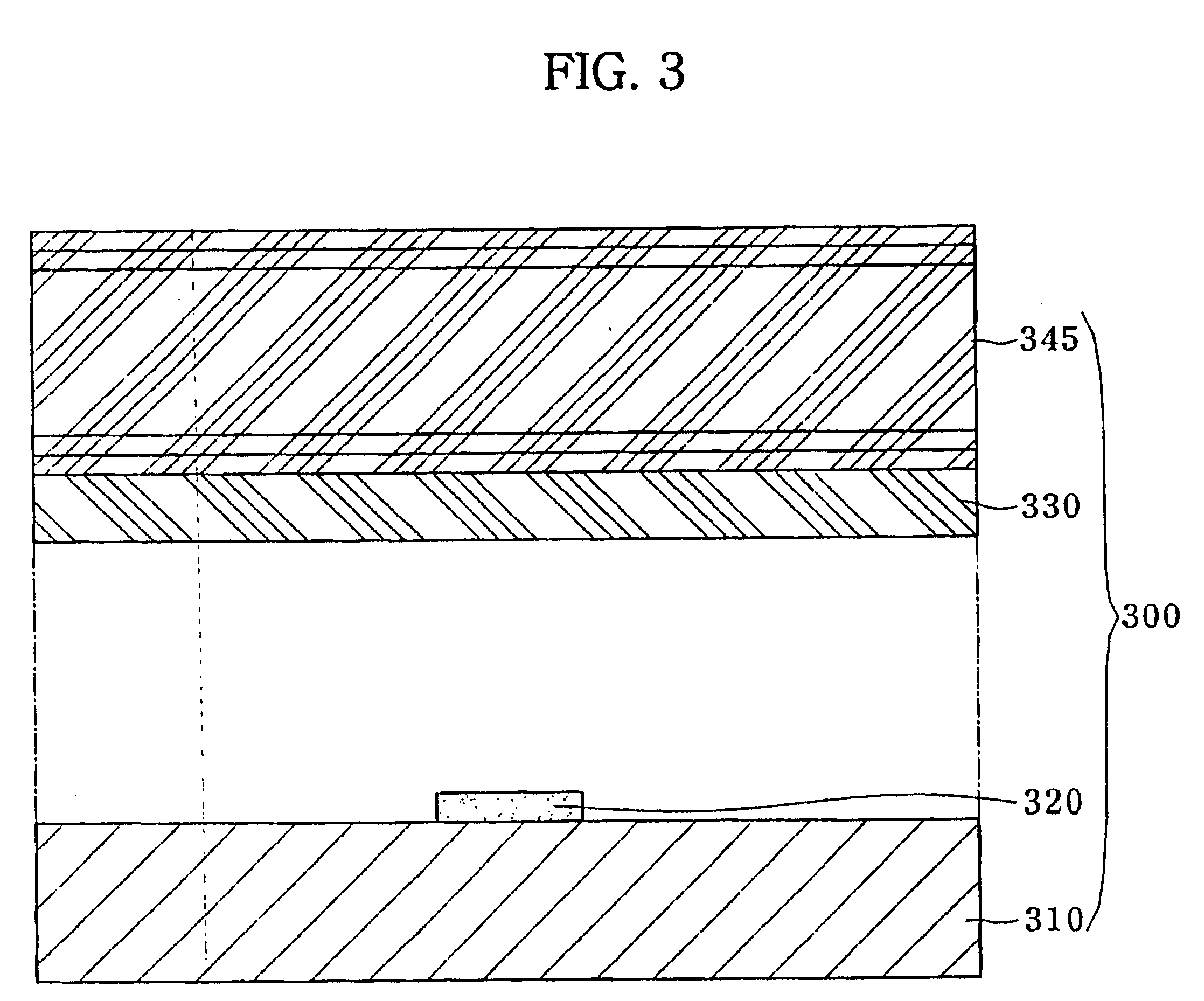
[0058]FIG. 3 is a sectional view of a rear plate of a plasma display panel according to the third embodiment of the present invention.
[0059] As shown, composition and characteristics of each functional layer of a rear plate according to the third embodiment of the present invention is the same as the composition and characteristics of each functional layer of the rear plate according to the second embodiment of the present invention. In description of only the differences between them, a dielectric layer 330 and barrier walls 345 are prepared in a shape of green tapes having a thickness of 10 to 30 μm and 100 to 180 μm, respectively, and are integrated with each other. Thereafter, the dielectric layer 330 is attached to upper surfaces of electrodes 320 and a glass substrate 310. Then, they are baked at a temperature above 400° C., so that the dielectric layer 330 and the barrier walls 345 are completed.
[0060] The other constructions according to the third embodiment are the same a...
PUM
| Property | Measurement | Unit |
|---|---|---|
| thickness | aaaaa | aaaaa |
| reflectance | aaaaa | aaaaa |
| particle diameter | aaaaa | aaaaa |
Abstract
Description
Claims
Application Information