
Photomask structures providing improved photolithographic process windows and methods of manufacturing same

a technology of photolithographic process window and photolithographic mask, which is applied in the field of photomask structure, can solve the problems of limiting the ability to use binary masks for lithographic printing of sub-wavelength features, lithographic process window, and becoming increasingly difficult to meet critical dimension requirements, etc., and achieves the effect of improving image contras

Inactive Publication Date: 2006-10-19
SAMSUNG ELECTRONICS CO LTD
View PDF4 Cites 21 Cited by
  • Summary
  • Abstract
  • Description
  • Claims
  • Application Information

AI Technical Summary

Benefits of technology

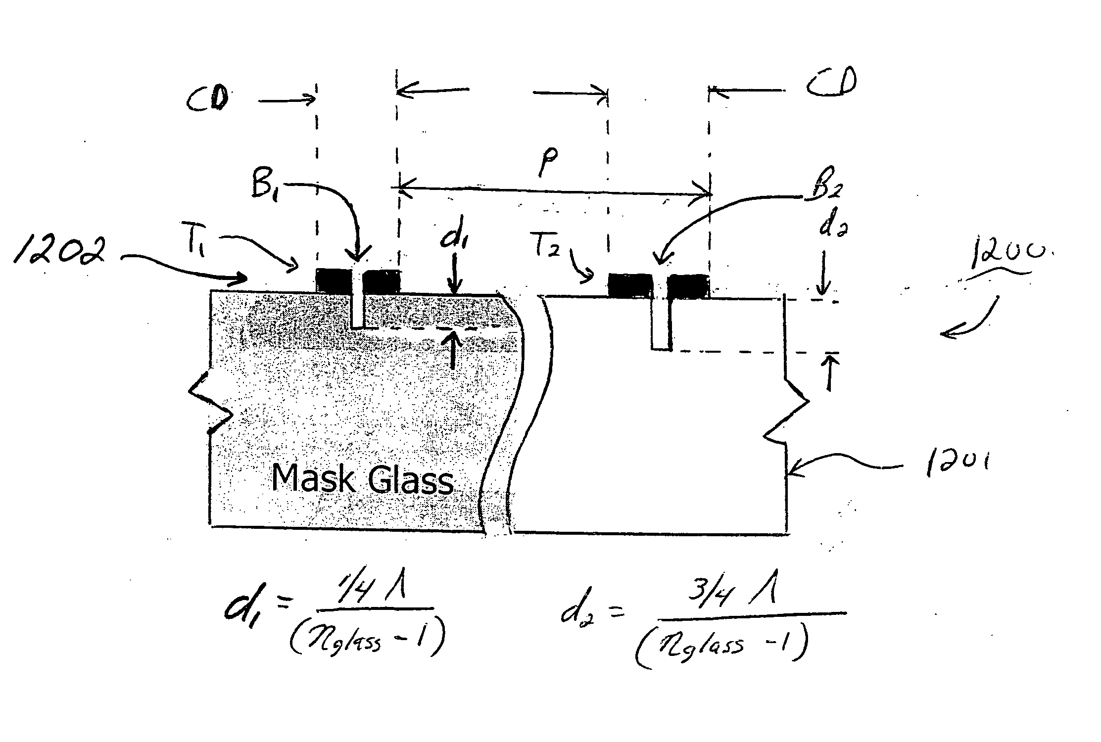
[0025] Exemplary embodiments of the invention generally include photomask structures that provide increased lithographic process windows for printing sub-wavelength features. In one exemplary embodiment of the invention, a photomask includes a mask substrate transparent to exposure light of a given wavelength, and a mask pattern formed on a surface of the substrate. The mask pattern comprises a printable element defined by a first and second critical edge, wherein the printable element includes an inner, non-printing feature formed between the first and second critical edges. The inner, non-printing feature is adapted to enhance image contrast at the first and second critical edges of the printable element for the given

Problems solved by technology

As feature patterns become increasing smaller (e.g., subwavelength features), however, it becomes increasingly difficult to meet critical dimension requirements as a result of optical proximity effects (OPE) which decrease the lithographic process window for printing sub-wavelength features.
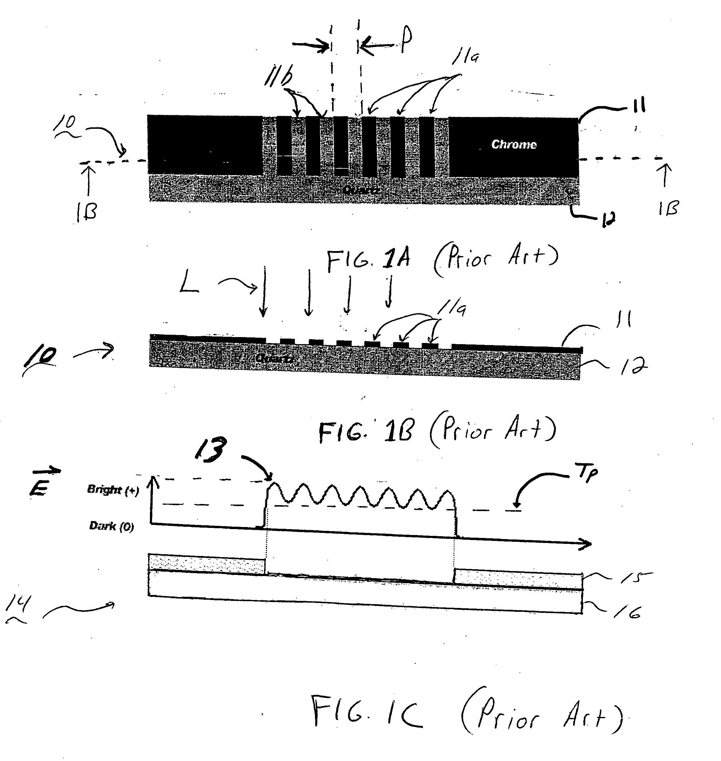
On the other hand, as compared to PSM structures, binary masks are generally known to be more susceptible to OPE due to diffraction, which limits the ability to use binary masks for lithographic printing of sub-wavelength features.
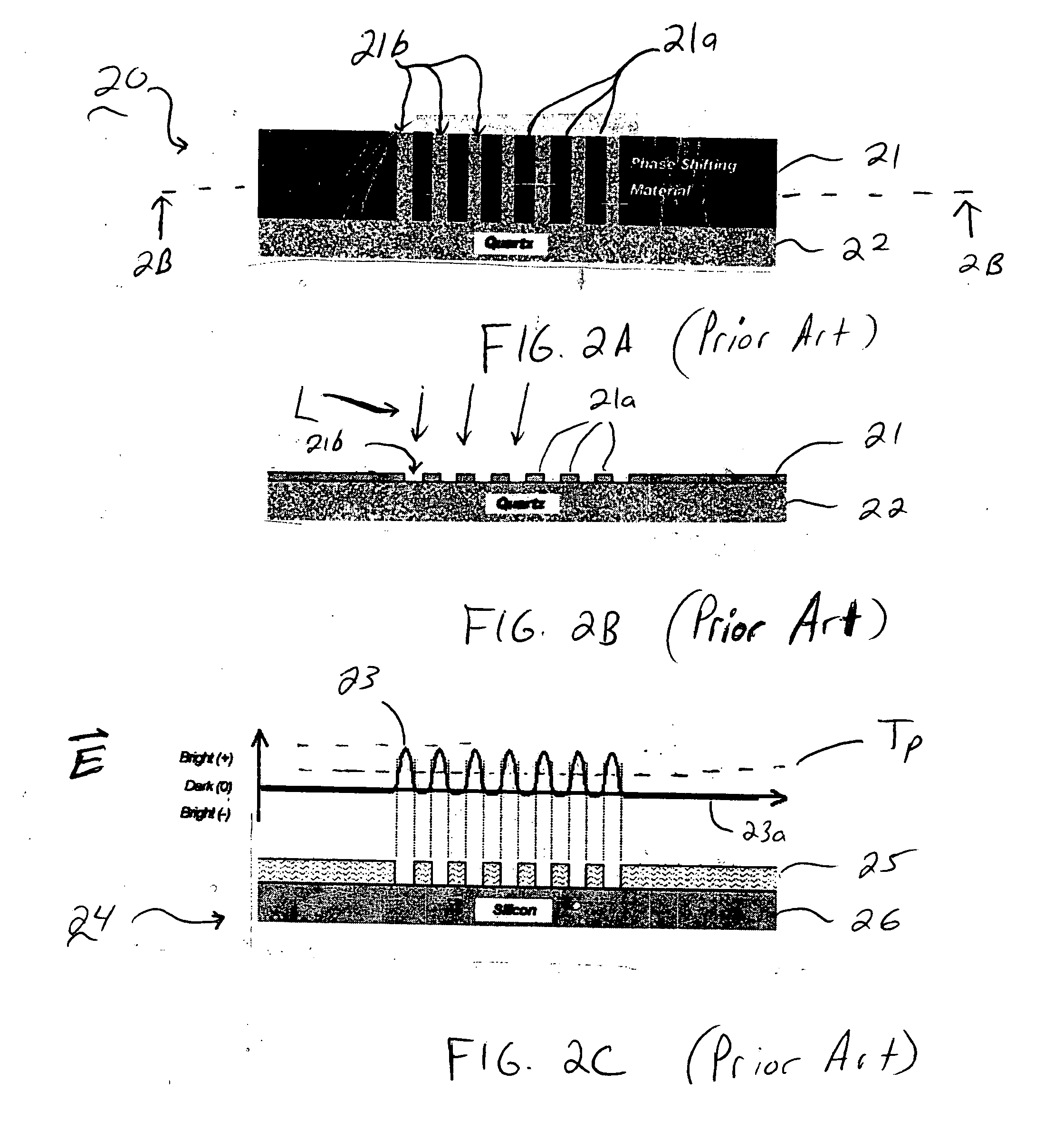
The resulting phase differences lead to DUV destructive interference, which improves image contrast.
Although enhancement techniques such as AAPSM and EAPSM discussed above can be utilized to improve resolution, such techniques can be complex, costly and can require increased chip size.
Moreover, PSM technology is subject to the “forbidden pitch” phenomenon, resulting in reduced process windows.
The forbidden pitch phenomenon has become a limiting factor in advanced photolithography for printing sub-wavelength features.
However, minor variations in parameters of the exposure process on photolithographic exposure equipment (scanners / steppers), may cause the critical dimensions (CD) of printed features to fall outside an acceptable manufacturing tolerances.
In this regard, the amount of defocus cannot be determined without an adequate method of measuring best focus.

Method used


Image

  • Photomask structures providing improved photolithographic process windows and methods of manufacturing same
  • Photomask structures providing improved photolithographic process windows and methods of manufacturing same
  • Photomask structures providing improved photolithographic process windows and methods of manufacturing same

Examples


Embodiment Construction

[0048] Exemplary photomask structures and methods for using photomask structures for improving lithographic process windows and enable focal point detection for fabricating such devices according to exemplary embodiments of the invention will now be described more fully with reference to the accompanying drawings. It is to be understood that the drawings are merely schematic depictions where the thickness and dimensions of various elements, layers and regions are not to scale, but rather exaggerated for purposes of clarity. It is to be further understood that when a layer is described herein as being “on” or “over” another layer or substrate, such layer may be directly on the other layer or substrate, or intervening layers may also be present. It is to be further understood that the same reference numerals used throughout the drawings denote elements that are the same or similar or have the same or similar functions.

[0049]FIGS. 5A and 5B schematically illustrate a photomask accordi...


PUM


Abstract

Photolithographic methods for semiconductor manufacturing are provided wherein photomask structures are designed to provide increased lithographic process windows for printing sub-wavelength features. In one aspect, a photomask includes a mask substrate transparent to exposure light of a given wavelength, and a mask pattern formed on a surface of the substrate. The mask pattern comprises a printable element defined by a first and second critical edge, wherein the printable element includes an inner, non-printing feature formed between the first and second critical edges. The inner, non-printing feature is adapted to enhance image contrast at the first and second critical edges of the printable element for the given wavelength of exposure light during a photolithographic process. The non-printing feature comprises a space feature that exposes a region of the mask substrate aligned to the printable element between the first and second critical edges, and a trench feature that is formed in the mask substrate and aligned to the space feature.

Description

CROSS-REFERENCE TO RELATED APPLICATIONS [0001] This application claims priority to U.S. Provisional Application Ser. Nos. 60 / 671,626 filed on Apr. 15, 2005, and 60 / 673,669 filed on Apr. 21, 2005, which are both fully incorporated herein by reference.TECHNICAL FIELD OF THE INVENTION [0002] The present invention relates generally to improved photolithographic methods for semiconductor manufacturing. In particular, the invention relates to photomask structures that provide increased lithographic process windows for printing sub-wavelength features. BACKGROUND [0003] Photolithography is an integral process in manufacturing semiconductor IC (integrated circuit) devices. In general, a photolithographic process includes coating a semiconductor wafer (or substrate) with a layer of photoresist, and exposing the photoresist with an actinic light source (such as an excimer laser, mercury lamp, etc.,) through a photomask having an image of an integrated circuit. For example, a lithographic tool...

Claims


Application Information

Patent Timeline
IPC IPC(8): G03C5/00G03F1/00
CPCG03F1/14G03F1/144G03F1/36G03F1/32G03F1/26G03F1/62G03F1/38
Inventor KIM, HO-CHUL
Owner SAMSUNG ELECTRONICS CO LTD
Learn More