Mbe growth of an algan layer or algan multilayer structure

a technology of mbe and algan, which is applied in the direction of crystal growth process, polycrystalline material growth, chemistry apparatus and processes, etc., can solve the problems of mbe growth of high quality nitride semiconductor layers, difficult to obtain v/iii ratio of 10:1 or greater during mbe growth of nitride semiconductor layers, and none of these documents addresses algan growth

Inactive Publication Date: 2006-10-26
SHARP KK
View PDF9 Cites 23 Cited by
  • Summary
  • Abstract
  • Description
  • Claims
  • Application Information

AI Technical Summary

Benefits of technology

[0028] The first (Al,Ga)N layer may have an aluminium mole fraction of...

Problems solved by technology

At present, growing high quality nitride semiconductor layers by MBE is more difficult than growing such layers by MOVPE.
The principal difficulty is in supplying sufficient nitrogen during the growth process, and it is difficult to obtain a V/III ratio of 10:1 or greater during MBE growth of a nitride semiconductor layer.
This prior technique gives prom...

Method used


Image

  • Mbe growth of an algan layer or algan multilayer structure
  • Mbe growth of an algan layer or algan multilayer structure
  • Mbe growth of an algan layer or algan multilayer structure

Examples


Embodiment Construction

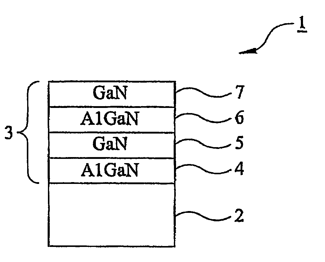
[0039]FIG. 1 is a schematic illustration of a semiconductor structure 1. Such a structure may be used in an optoelectronic device such as a light-emitting device, for example a light-emitting diode (“LED”) or a laser diode. The structure 1 has a substrate 2. The substrate may be a bulk substrate of Ga or InGaN. The substrate may alternately consist of an epitaxial layer of GaN or InGaN disposed on a base substrate of, for example, sapphire, SiC, Si, ZnO, MgO or GaN.

[0040] The semiconductor structure 1 of FIG. 1 further comprises a semiconductor multilayer structure 3. The multilayer structure 3 consists of a plurality of (Al,Ga)N layers having at least two different aluminium mole fractions. Four (Al,Ga)N layers are shown in FIG. 1, but a multilayer structure may consist of fewer or more than four (Al,Ga)N layers. In the structure shown in FIG. 1 the first (Al,Ga)N layer 4 of the multilayer structure 3 is an AlGaN layer (that is, it has a non-zero aluminium mole fraction). The seco...


PUM


Abstract

A method of growing an AlGaN semiconductor layer structure by Molecular Beam Epitaxy comprises supplying ammonia, gallium and aluminium to a growth chamber thereby to grow a first (Al,Ga)N layer by MBE over a substrate disposed in the growth chamber. The first (Al,Ga)N layer has a non-zero aluminium mole fraction. Ammonia is supplied at a beam equivalent pressure of at least 1 10−4 mbar, gallium is supplied at a beam equivalent pressure of at least 1 10−8 mbar and aluminium is supplied at a beam equivalent pressure of at least 1 10−8 mbar during the growth step. Once the first (Al,Ga)N layer has been grown, varying the supply rate of gallium and/or aluminium enables a second (Al,Ga)N layer, having a different aluminium mole fraction from the first (Al,Ga)N layer to be grown by MBE over the first (Al,Ga)N layer. This process may be repeated to grown an (Al,Ga)N multilayer structure.

Description

TECHNICAL FIELD [0001] This invention relates to a molecular beam epitaxy (MBE) method for the epitaxial growth of an AlGaN layer. The invention may be applied to the epitaxial growth of a semiconductor layer structure, for example a quantum well or multiple quantum well structure, comprising one or more AlxGa1-xN (0≦x≦1) layers. The layer structure may be incorporated in a semiconductor light-emitting device. BACKGROUND ART [0002] The term “AlGaN” is used to denote a member of the AlxGa1-xN (0≦x≦1) material family having an aluminium mole fraction x that is non-zero but is less than 1. The complete material family, including x=0 and x=1, will be referred to herein as “(Al,Ga)N” for convenience. [0003] Similarly, the term “InGaN” is used to denote a member of the InyGa1-yN (0≦y≦1) material family having an aluminium mole fraction y that is non-zero but is less than 1. The complete material family, including y=0 and y=1, will be referred to herein as “(In,Ga)N” for convenience. [0004...

Claims


Application Information

Patent Timeline
IPC IPC(8): H01L29/20H01L21/20H01L29/06C30B23/02H01L21/203
CPCC30B23/02C30B29/403C30B29/406H01L21/0237H01L21/02631H01L21/02458H01L21/0254H01L21/0262H01L21/02389
Inventor BOUSQUET, VALERIEHOOPER, STEWART EDWARDBARNES, JENNIFER MARYJOHNSON, KATHERINE L.HEFFERNAN, JONATHAN
Owner SHARP KK
Why Eureka
Try Eureka