Display device and method for manufacturing the same

Inactive Publication Date: 2006-10-26
SHARP KK
12 Cites 74 Cited by

AI-Extracted Technical Summary

Problems solved by technology

In particular when the final size of a device is required to be small, the slimming down of the liquid crystal display panel 100 as one of the components thereof is a very important issue.
Therefore, even though the other components are downsized, dramatic size reduction of the device cannot be expected unless the size of the liquid crystal display panel 100 is reduced.
As a result, the strength of the glass substrates 101 and 102 decreases, thereby inevitably impairing the reliability of the liquid crystal display device (resistance against vibr...

Benefits of technology

[0041] If the glass substrate of the first substrate and the glass substrate of the second substrate have different initial thicknesses and the same etch rate, the total thickn...

Abstract

A liquid crystal display device includes: an active matrix substrate including a glass substrate; a counter substrate which is arranged to face the active matrix substrate and includes a glass substrate which is thinner than the glass substrate of the active matrix substrate; and a display medium layer which is provided between the active matrix substrate and the counter substrate. The rate at which the glass substrate of the active matrix substrate is etched by an etching solution is lower than the rate at which the glass substrate of the counter substrate is etched by the etching solution.

Application Domain

Non-linear optics

Technology Topic

Liquid-crystal displayMedia layer +2

Image

  • Display device and method for manufacturing the same
  • Display device and method for manufacturing the same
  • Display device and method for manufacturing the same

Examples

  • Experimental program(4)

Example

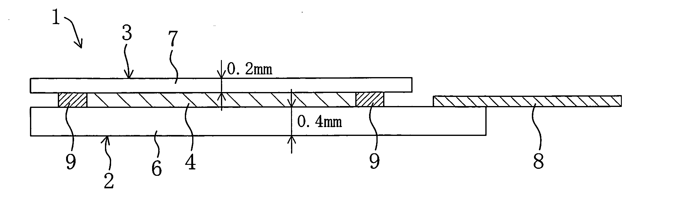
[0052] FIGS. 1 to 5 show a first embodiment of the present invention.
[0053]FIG. 1 is a sectional view schematically illustrating a liquid crystal display device 1 as a display device of the present invention. As shown in FIG. 1, the liquid crystal display device 1 includes an active matrix substrate 2 as a first substrate, a counter substrate 3 as a second substrate facing the active matrix substrate 2 and a liquid crystal layer 4 as a display medium layer provided between the substrates 2 and 3.
[0054] The active matrix substrate 2 includes a glass substrate 6 and a plurality of thin film transistors (not shown and abbreviated as TFTs) which are formed on the surface of the glass substrate 6 facing the liquid crystal layer 4. The active matrix substrate 2 further includes a plurality of pixels arranged in a matrix. The TFTs are provided on a pixel-by-pixel basis.
[0055] The thickness of the glass substrate 6 is 0.4 mm, for example. An orientation film (not shown) is formed on the surface of the glass substrate 6 facing the liquid crystal layer 4 to cover the TFTs. A polarizing plate (not shown) is stacked on the other surface of the glass substrate 6 not facing the liquid crystal layer 4.
[0056] A driver (not shown) for driving and controlling the TFTs is also formed on the glass substrate 6. The TFTs are connected to the driver through signal wires and scanning wires which are not shown in the drawings. The TFTs and the driver include semiconductor elements made of low-temperature polysilicon, for example.
[0057] As shown in FIG. 1, a flexible printed substrate 8 is mounted on the active matrix substrate 2. The flexible printed substrate 8 is connected to the driver and supplies a drive signal to the driver.
[0058] The counter substrate 3 includes a glass substrate 7. A color filter and shared electrodes made of ITO (not shown) are formed on the surface of the glass substrate 7 facing the liquid crystal layer 4. The thickness of the glass substrate 7 is 0.2 mm, for example, which is smaller than the thickness of the glass substrate 6 of the active matrix substrate 2. An orientation film (not shown) is formed on the surface of the glass substrate 7 facing the liquid crystal layer 4 to cover the color filter and the shared electrodes. A polarizing plate (not shown) is formed on the other surface of the glass substrate 7 not facing the liquid crystal layer 4.
[0059] The active matrix substrate 2 and the counter substrate 3 are bonded to each other with a spacer (not shown) and a sealing member 9 sandwiched therebetween. A certain gap is formed between the active matrix substrate 2 and the counter substrate 3, in which liquid crystal material is sealed to form the liquid crystal layer 4. Thus, the liquid crystal display device 1 is configured such that the driver and the TFTs control the orientation of the liquid crystal molecules in the liquid crystal layer 4 on the pixel-by-pixel basis, thereby producing a desired display.
[0060] As a characteristic of the present invention, the rate at which the glass substrate 6 of the active matrix substrate 2 is etched by an etching solution containing hydrogen fluoride is lower than the rate at which the glass substrate 7 of the counter substrate 3 is etched by the same etching solution. The glass substrate 6 is made thicker than the glass substrate 7 and therefore has higher mechanical strength than that of the glass substrate 7.
---Manufacturing Method---
[0061] Next, an explanation of a method for manufacturing the liquid crystal display device 1 will be provided. The method includes the steps of bonding the substrates, etching the substrates and mounting the flexible printed substrate.
[0062] First, in the step of bonding the substrates, TFTs, pixel electrodes, signal wires, scanning wires and a driver, which are not shown in the drawings, are formed on a glass substrate 6 as a component of an active matrix substrate 2. The TFTs and the driver include elements made of low-temperature polysilicon.
[0063] On a glass substrate 7 as a component of a counter substrate 3, a color filter and shared electrodes which are not shown in the drawings are formed. An orientation film is then formed thereon to cover the color filter and the shared electrodes. The glass substrates 6 and 7 are bonded together with a spacer and a sealing member 9 sandwiched therebetween. Then, liquid crystal material is sealed in a gap formed between the glass substrates 6 and 7 to form a liquid crystal layer 4. Before etching, the glass substrates 6 and 7 have the same thickness of 0.7 mm as shown in FIG. 2. The reason why the initial thicknesses of the glass substrates 6 and 7 are set to 0.7 mm is that it is the usual thickness employed in the manufacture line and hence the substrates are easily handled.
[0064] Next, in the step of etching the substrates, the bonded glass substrates 6 and 7 are immersed in an etching solution containing hydrogen fluoride. Specifically, the glass substrates 6 and 7 are etched for the same period of time. In this step, each of the glass substrates 6 and 7 is thinned down. The etch rates of the glass substrates 6 and 7 in the etching solution are varied such that the glass substrate 6 is etched more slowly than the glass substrate 7. Therefore, as shown in FIG. 3, the glass substrate 6 is etched by a smaller amount to reduce the thickness to 0.4 mm, while the glass substrate 7 is etched by a larger amount to reduce the thickness to 0.2 mm. As a result, the mechanical strength of the glass substrate 6 becomes higher than that of the glass substrate 7. Then, polarizing plates are deposited on the outside surfaces of the glass substrates 6 and 7, respectively.
[0065] Next, in the step of mounting the flexible printed substrate, a flexible printed substrate 8 is mounted on the active matrix substrate 2 including the etched glass substrate 6. Thus, through the above-described steps, the liquid crystal display device 1 is fabricated.
---Effect of the First Embodiment---
[0066] The flexible printed substrate 8 is press-mounted on the active matrix substrate 2. Therefore, the active matrix substrate 2 needs to have enough mechanical strength to endure the pressure applied thereto in the mounting step. The counter substrate 3 does not require such a mechanical strength. According to the present embodiment, even if the initial thicknesses of the glass substrates 6 and 7 before etching are the same, the active matrix substrate 2 which requires certain mechanical strength is made relatively thick, while the counter substrate 3 which does not require such a mechanical strength is made relatively thin by etching. Therefore, the total thickness of the active matrix substrate 2 and the counter substrate 3 are reduced. As a result, the liquid crystal display device 1 is slimmed down. Since the glass substrates 6 and 7 have the same thickness before etching, the substrates are easily handled in the manufacture line and can be worked with existing manufacturing facilities.
[0067] Moreover, as the slimming down of the resulting device is achieved by single immersion of the glass substrates 6 and 7 in the etching solution, the manufacturing steps are simplified. Therefore, reduction in production cost and improvement in yield are expected.
[0068] If amorphous silicon is used to form the TFTs and the driver, the driver must be mounted on the flexible printed substrate 8. As a result, the flexible printed substrate 8 including the driver inevitably becomes thick. Therefore, even if the glass substrates 6 and 7 are thinned down, the thickness of the device cannot be easily reduced due to the thick flexible printed substrate 8. In the present embodiment, however, low-temperature polysilicon is used to form the TFTs and the driver. Therefore, the driver is formed on the glass substrate 6 without significant increase in substrate thickness and the resulting device is effectively slimmed down.
[0069] As shown in FIG. 4, the thickness of the glass substrate 6 of the active matrix substrate 2 may be set to 0.5 mm and the thickness of the glass substrate 7 of the counter substrate 3 may be set to 0.1 mm. With these thicknesses, the thickness of the resulting device is kept about 0.6 mm and the mechanical strength of the glass substrate 6 is enhanced.
[0070] If it is difficult to control the final thicknesses of the glass substrates 6 and 7 by merely adjusting the etch rates, the thicknesses of the glass substrates 6 and 7 may be adjusted before etching.

Example

EXAMPLE
[0071] Now, an explanation of a specific example of the present invention will be provided.
[0072] A glass substrate A (AN100 manufactured by ASAHI GLASS) was used as the glass substrate 6 of the active matrix substrate 2 and a glass substrate B (1737 manufactured by Corning) was used as the glass substrate 7 of the counter substrate 3. Under certain etching conditions, the etch rate of the glass substrate A is 4.4 μm/min and that of the glass substrate B is 5.2 μm/min.
[0073] Elements such as TFTs and wires were formed on the glass substrate A and a color filter and other elements were formed on the glass substrate B. Then, the glass substrates A and B are bonded together. The bonded substrates were immersed in an etching solution containing hydrogen fluoride under the above-described conditions to etch the substrates for about 42 minutes. As shown in Table 1, the thicknesses of the glass substrates A and B after the 42-minute etching were 0.52 mm and 0.48 mm, respectively. TABLE 1 Time (minute) 0 42 84 Thickness of glass 0.7 0.52 0.34 substrate A (mm) Thickness of glass 0.7 0.48 0.26 substrate B (mm)+UZ,20/23 +UZ,26/29 Total thickness 1.4 1.00 0.6 (mm)
[0074] The etching was continued for another 42 minutes. Then, as shown in Table 1, the thickness of the glass substrate A was reduced to 0.34 mm and that of the glass substrate B was reduced to 0.26 mm. FIG. 5 shows a graph illustrating the variations in thicknesses of the glass substrates A and B. FIG. 5 indicates that the thicknesses of the glass substrates A and B are linearly reduced with time. From the obtained results, it is found that if each of the glass substrates A and B has an initial thickness of 1.1 mm and the etching is carried out for 166 minutes, the thicknesses of the glass substrates A and B are reduced to 0.37 mm and 0.23 mm, respectively, thereby obtaining a desired device having a thickness of about 0.6 mm.

Example

Second Embodiment
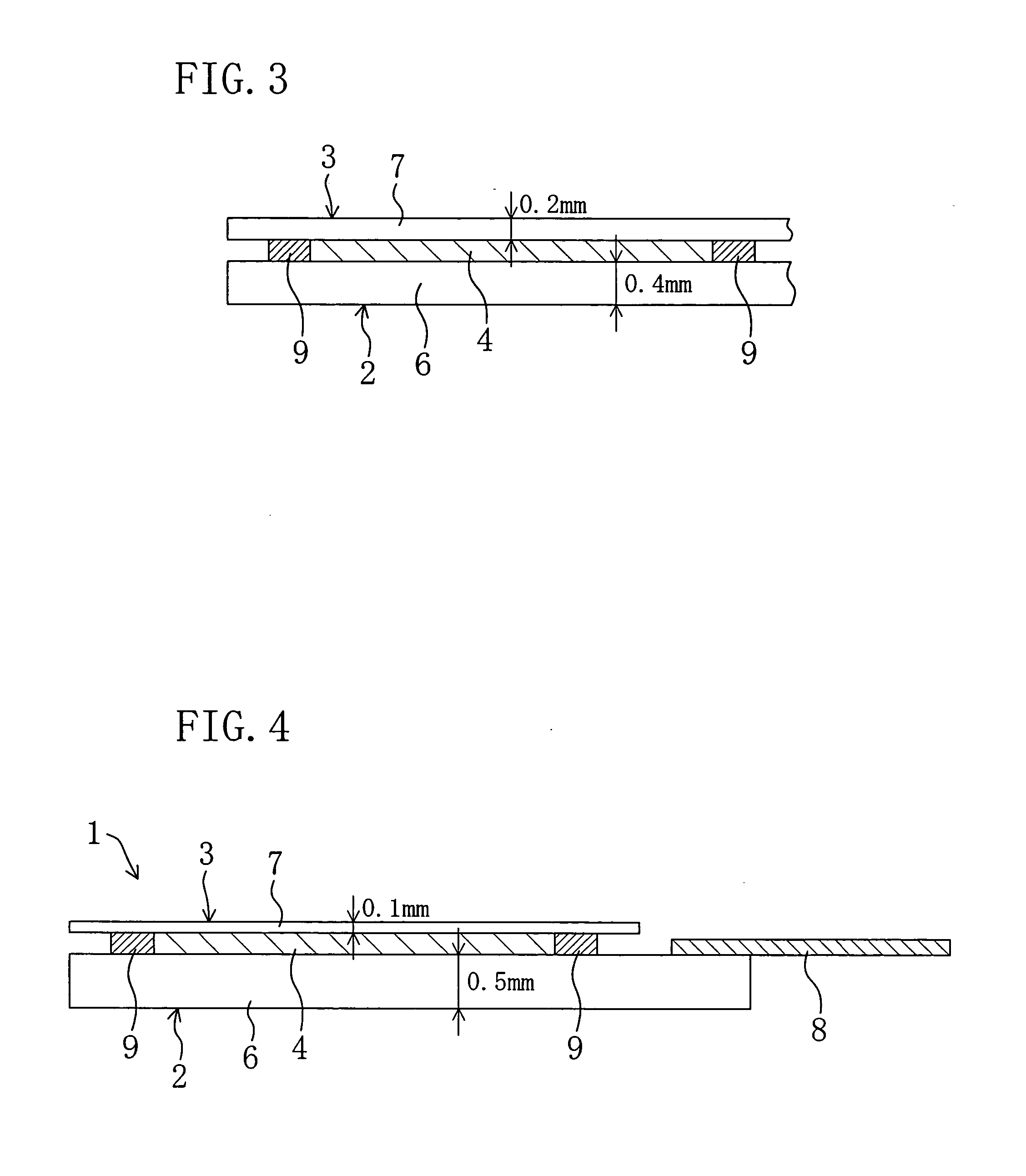
[0075]FIG. 6 shows a second embodiment of the present invention. In the following embodiments, the same components as those shown in FIGS. 1 to 4 are indicated by the same reference numerals to omit a detailed explanation.
[0076] A liquid crystal display device 1 of the present embodiment includes an active matrix substrate 2, a counter substrate 3 and a liquid crystal layer 4 as shown in FIG. 6. The active matrix substrate 2 includes a 0.5 mm thick glass substrate 6. The counter substrate 3 includes a 0.1 mm thick plastic substrate 10. In other words, the liquid crystal display device 1 includes the glass substrate 6 and the plastic substrate 10 which is provided to face the glass substrate 6 and thinner than the glass substrate 6.
[0077] In order to fabricate the liquid crystal display device 1 described above, first, in the step of bonding the substrates, a color filter (a coloring layer), TFTs, pixel electrodes, signal wires, scanning wires and a driver which are not shown in the drawings are formed on the glass substrate 6 as a component of the active matrix substrate 2. Then, an orientation film is formed thereon. The TFTs and the driver include elements made of low-temperature polysilicon. The thickness of the glass substrate 6 before etching is 0.7 mm, for example.
[0078] Shared electrodes and other elements which are not shown in the drawings are formed on the plastic substrate 10 as a component of the counter substrate 3. The thickness of the plastic substrate 10 is 0.1 mm, for example. Then, the glass substrate 6 and the plastic substrate 10 are bonded together and a liquid crystal layer 4 is formed therebetween in the same manner as described in the first embodiment.
[0079] In this embodiment, the color filter is formed not on the counter substrate 3 but on the active matrix substrate 2. Therefore, the liquid crystal display device 1 is achieved with accuracy irrespective of different thermal expansion coefficients of glass and plastic.
[0080] Then, in the step of etching the substrates, the glass substrate 6 and the plastic substrate 10 bonded to each other are immersed in an etching solution containing hydrogen fluoride. At this time, only the glass substrate 6 is etched, but the plastic substrate 10 is not etched. As a result, the thickness of the glass substrate 6 is reduced to 0.5 mm, for example. The glass substrate 6 is kept thicker than the plastic substrate 10. The subsequent steps are the same as those described in the first embodiment. Thus, the liquid crystal display device 1 is fabricated.
---Effect of the Second Embodiment---
[0081] According to the second embodiment, the glass substrate 6 and the plastic substrate 10 are used as a pair of substrates. Therefore, only the glass substrate 6 is etched, while the plastic substrate 10 is not etched. As the mechanical strength of the plastic substrate 10 required in the manufacture line is not so important, the plastic substrate 10 may be made thin from the start. Therefore, the liquid crystal display device 1 is easily slimmed down.

PUM

no PUM

Description & Claims & Application Information

We can also present the details of the Description, Claims and Application information to help users get a comprehensive understanding of the technical details of the patent, such as background art, summary of invention, brief description of drawings, description of embodiments, and other original content. On the other hand, users can also determine the specific scope of protection of the technology through the list of claims; as well as understand the changes in the life cycle of the technology with the presentation of the patent timeline. Login to view more.

Similar technology patents

Rotary damper

InactiveUS20050252740A1reduce thickness
Owner:SOMIC ISHIKAWA INC

Direct downward background module

InactiveCN1510482Areduce thickness
Owner:BENQ CORP

Thin film ink jet printhead adhesion enhancement

InactiveUS20050078151A1increase adhesionreduce thickness
Owner:FUNAI ELECTRIC CO LTD

Heat exchanger

Owner:DENSO CORP

Method for mfg. organic electroluminescent display panel covered with protective film

InactiveCN1452437Areduce thicknessovercome manufacturing difficulties
Owner:朱星厚 +2

Classification and recommendation of technical efficacy words

Why Eureka
Try Eureka