Trench gate type semiconductor device

a technology of trench gate and semiconductor, applied in the direction of semiconductor devices, basic electric elements, electrical equipment, etc., can solve the problems of trench gate type mosfet breakdown, device damage, etc., and achieve the effect of reducing surge voltage and small current cutoff speed

Inactive Publication Date: 2006-11-02
DENSO CORP
View PDF8 Cites 5 Cited by
  • Summary
  • Abstract
  • Description
  • Claims
  • Application Information

AI Technical Summary

Benefits of technology

[0013] In the above device, the electric field concentration is generated at the bottom of the trench in a positive manner when the IGBT is switched off. Thus, when the IGBT is switched off, the avalanche current flows by means of the electric field concentration at the bottom of the trench, so that the current cutoff speed becomes small. Thus, the surge voltage is reduced so that the device has a small surge voltage when the IGBT is switched off.

Problems solved by technology

However, when this method is used for the IGBT, the following problems occur.
Specifically, when the IGBT is used for switching with large current such as 400 Ampere in order to drive an inductance load, the problems occur.
Further, when the surge voltage exceeds a yielding voltage of the device, and when the absorbed energy of the device exceeds a breakdown energy, the device may be damaged.
Furthermore, the breakdown may be occurred in a trench gate type MOSFET.

Method used


Image

  • Trench gate type semiconductor device
  • Trench gate type semiconductor device
  • Trench gate type semiconductor device

Examples


first embodiment

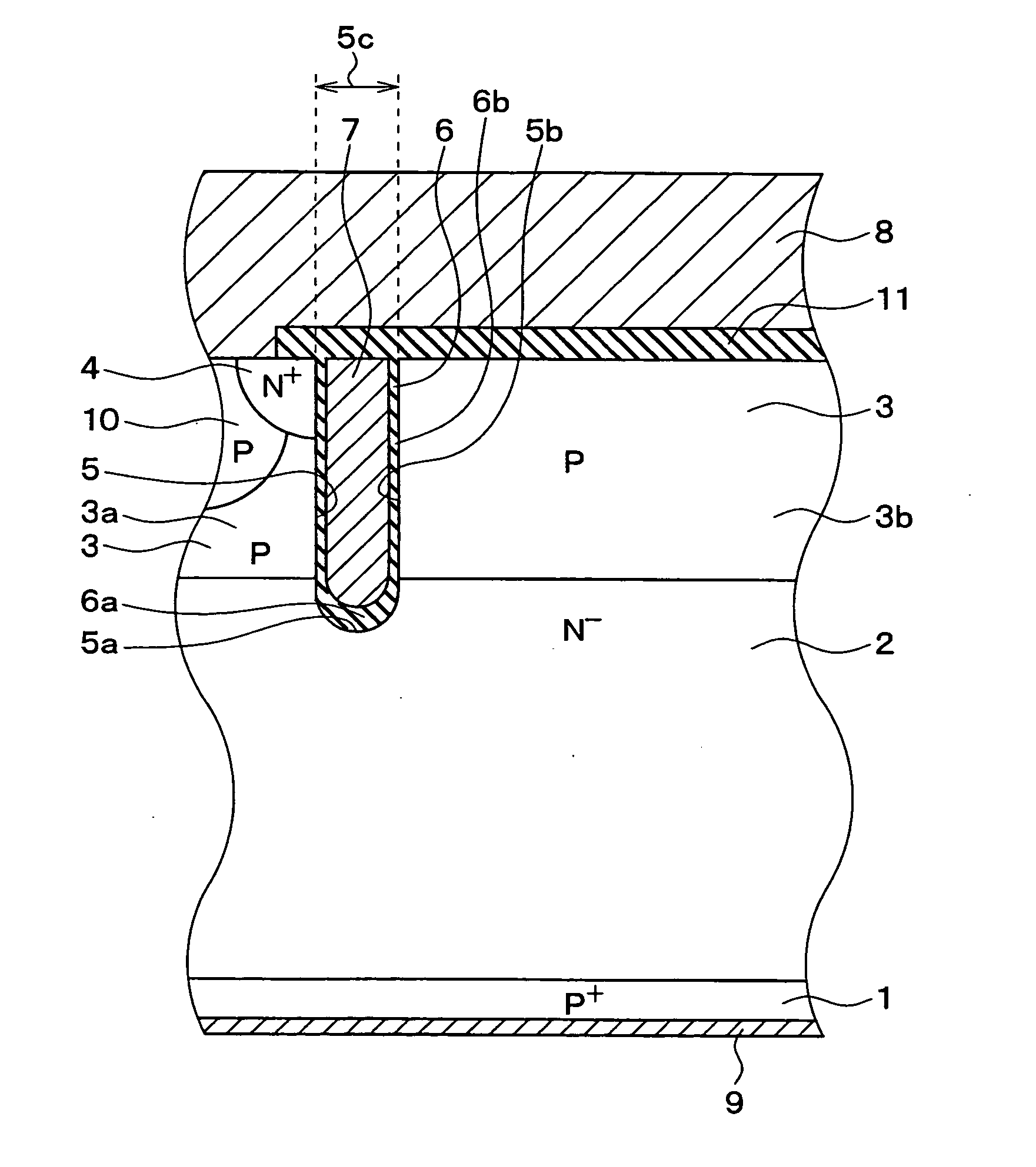
[0037] In view of the above points, an IGBT as a semiconductor device according to a first embodiment of the present invention is provided. The IGBT is shown in FIG. 1. The IGBT is used for driving an inductance load. For example, the IGBT is used for switching with large current such as 400 Ampere.

[0038] Here, in the IGBT shown in FIG. 1, a P type conductivity represents a first type conductivity, a N type conductivity represents a second type conductivity, a P+ type layer 1 represents a first semiconductor layer, a N− type drift layer 2 represents a second semiconductor layer, a P type base region 3 represents a third semiconductor layer, a N+ type emitter region 4 represents a fourth semiconductor layer, an emitter electrode 8 represents a first electrode, and a collector electrode 9 represents a second electrode.

[0039] The P+ type layer 1 is made of, for example, silicon substrate. A gate insulation film 6 is made of, for example, silicon oxide film (i.e., SiO2 film). Further,...

example no.1

EXAMPLE NO. 1

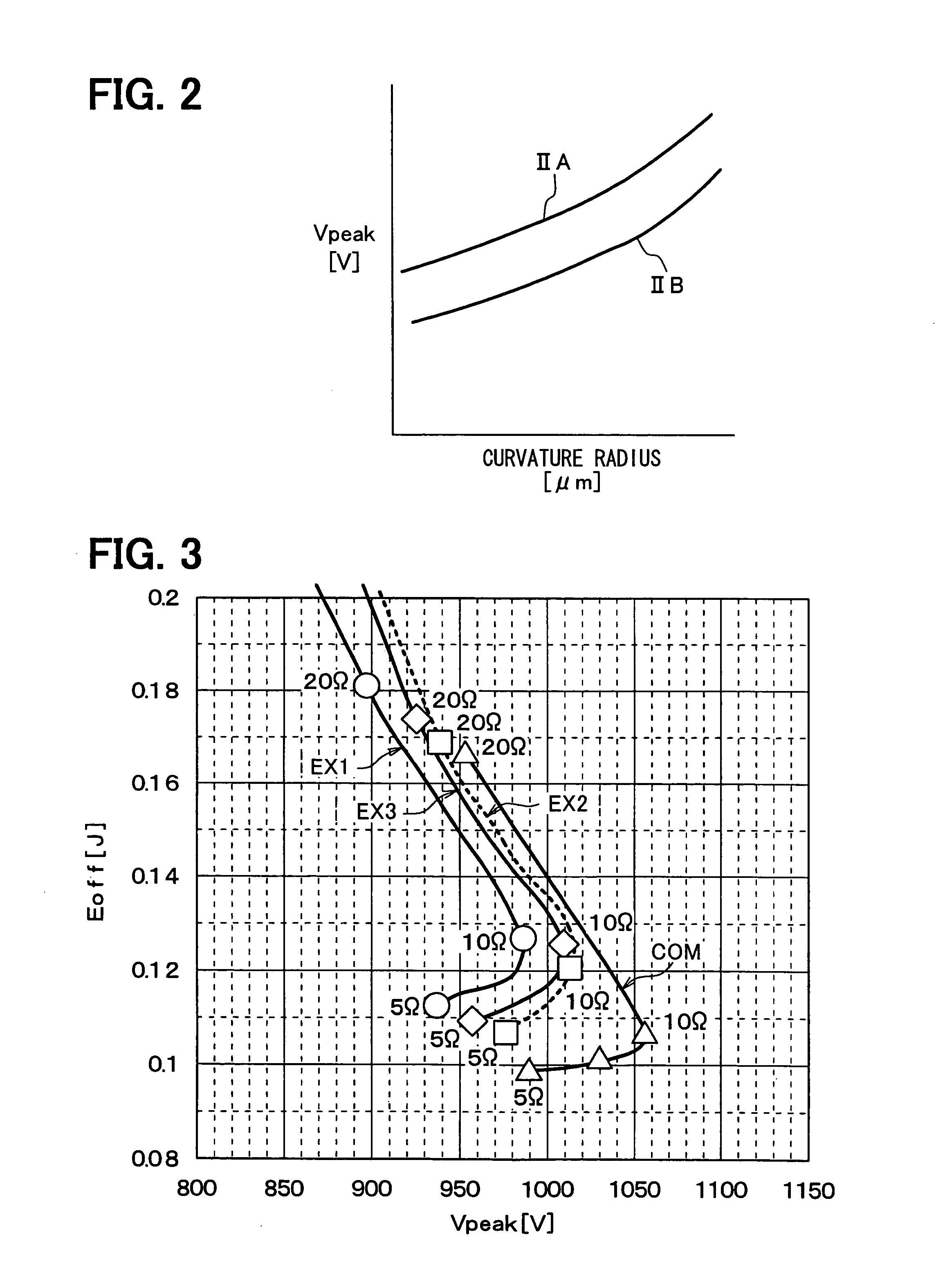
[0060] The curvature radius of the bottom 5a of the trench 5 is 0.5 μm. The thickness of the bottom part 6a of the gate insulation film 6 is 2⁢12

times larger than that of the side part 6b. Specifically, the thickness of the bottom part 6a of the gate insulation film 6 is 250 nm, and the thickness of the side part 6b of the gate insulation film 6 is 100 nm. The trench width 5c of the trench 5 is 0.8 μm, and a trench depth of the trench 5 is 5.0 μm. The thickness of the P+ type layer 1 is 145 μm. The threshold voltage is 6.4 Volts.

example no.2

EXAMPLE NO. 2

[0061] The curvature radius of the bottom 5a of the trench 5 is 0.5 μm. The thickness of the gate insulation film 6 is homogeneous. Specifically, the thickness of the gate insulation film 6 is 100 nm. The trench width 5c of the trench 5 is 0.8 μm, and a trench depth of the trench 5 is 5.0 μm. The thickness of the P+ type layer is 145 μm. The threshold voltage is 6.4 Volts.


PUM


Abstract

A semiconductor device includes: a first semiconductor layer; a second semiconductor layer on the first semiconductor layer; a third semiconductor layer on the second semiconductor layer; a fourth semiconductor layer in a part of the third semiconductor layer; a trench penetrating the fourth semiconductor layer and the third semiconductor layer and reaching the second semiconductor layer; a gate insulation film on an inner wall of the trench; a gate electrode on the gate insulation film in the trench; a first electrode; and a second electrode. The trench includes a bottom with a curved surface having a curvature radius equal to or smaller than 0.5 μm.

Description

CROSS REFERENCE TO RELATED APPLICATIONS [0001] This application is based on Japanese Patent Applications No. 2005-132220 filed on Apr. 28, 2005, and No. 2006-18580 filed on Jan. 27, 2006, the disclosures of which are incorporated herein by reference. FIELD OF THE INVENTION [0002] The present invention relates to a trench gate type semiconductor device. BACKGROUND OF THE INVENTION [0003] A trench gate type semiconductor device such as an insulated gate bipolar transistor (i.e., IGBT) and a MOS field effect transistor (i.e., MOSFET) is well known. For example, a trench gate type IGBT is disclosed in U.S. Pat. No. 6,737,705. The IGBT has a cell skipping structure. Specifically, some cell regions are periodically skipped to arrange in the IGBT so that an on-state voltage is reduced. Here, in general IGBT, multiple cell regions are serially arranged in the IGBT. Each cell region functions as an element. [0004] In the IGBT having the cell skipping structure, the thickness of a gate insula...

Claims


Application Information

Patent Timeline
Patent Type & Authority Applications(United States)
IPC IPC(8): H01L29/76
CPCH01L29/1095H01L29/42376H01L29/7397H01L2924/0002H01L2924/00
Inventor TSUZUKI, YUKIOTOKURA, NORIHITOOZEKI, YOSHIHIKOYAMAMOTO, KENSAKU
Owner DENSO CORP
Why Eureka
Try Eureka