Line scan sequential lateral solidification of thin films

a lateral solidification and line scan technology, applied in the field of thin film material processing, can solve the problems of limited ela and sls techniques, slightly different performance in the regions, etc., and achieve the effects of reducing the effect of differing energy fluence and energy densities of consecutive beam pulses, reducing sharpness, and reducing the effect of different energy fluence and energy densities

Active Publication Date: 2006-11-16
THE TRUSTEES OF COLUMBIA UNIV IN THE CITY OF NEW YORK
View PDF99 Cites 84 Cited by
  • Summary
  • Abstract
  • Description
  • Claims
  • Application Information

AI Technical Summary

Benefits of technology

[0008] Semiconductor film substrates are crystallized in a process that reduces the effect of differing energy fluences and energy densities of consecutive beam pulses on neighboring regions of a semiconductor film. The reduced effect provides films that can be used LCD and OLED displays that have greater uniformity and reduced sharpness in transition from adjacent crystallized regions.

Problems solved by technology

However, conventional ELA and SLS techniques are limited by variation in the laser pulses from one shot to the next.
In turn, this can cause slightly different performance in the regions of recrystallized film across the area of the display.

Method used


Image

  • Line scan sequential lateral solidification of thin films
  • Line scan sequential lateral solidification of thin films
  • Line scan sequential lateral solidification of thin films

Examples


Embodiment Construction

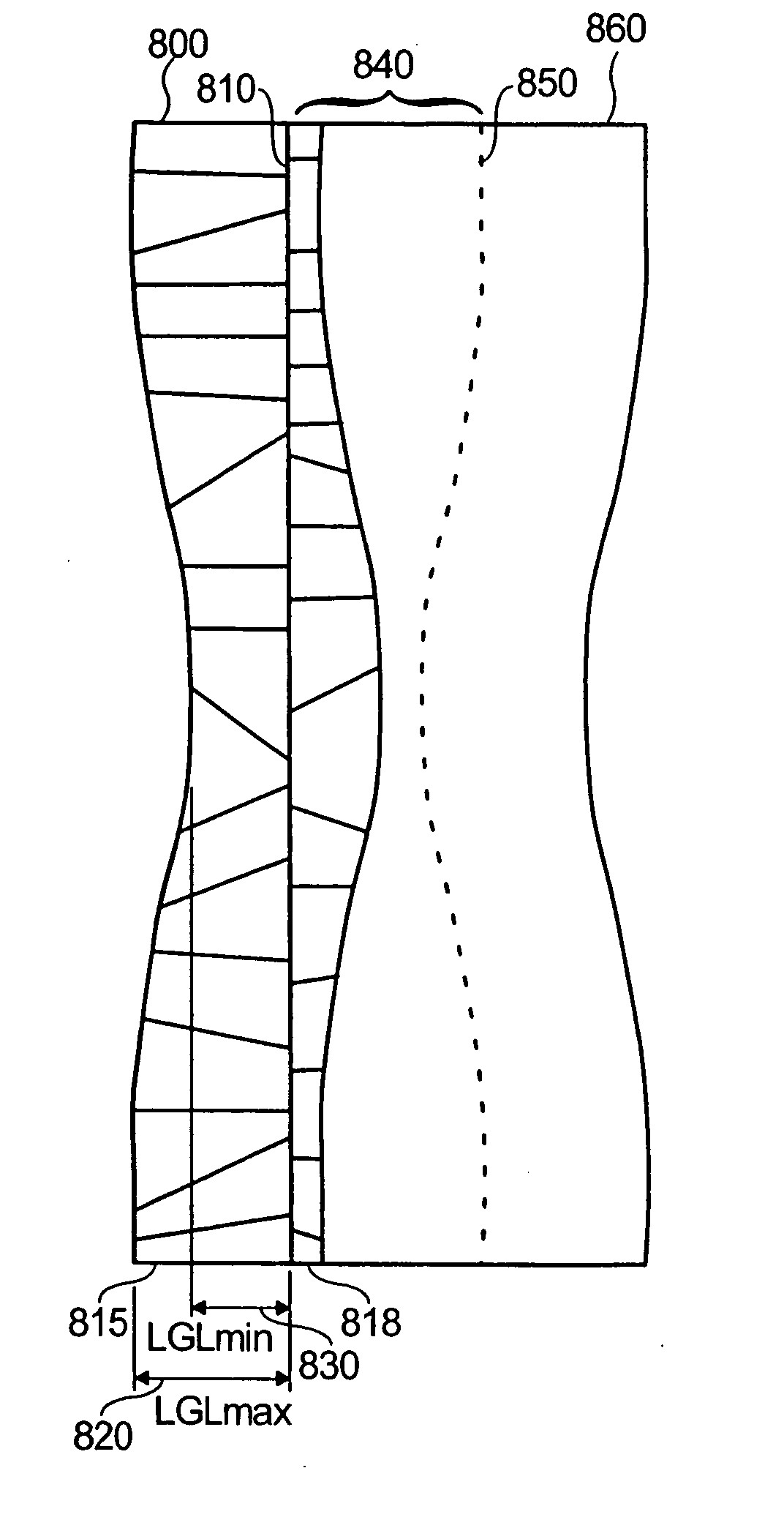
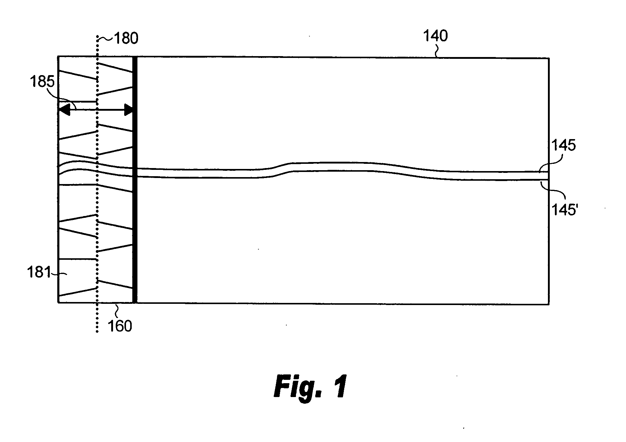
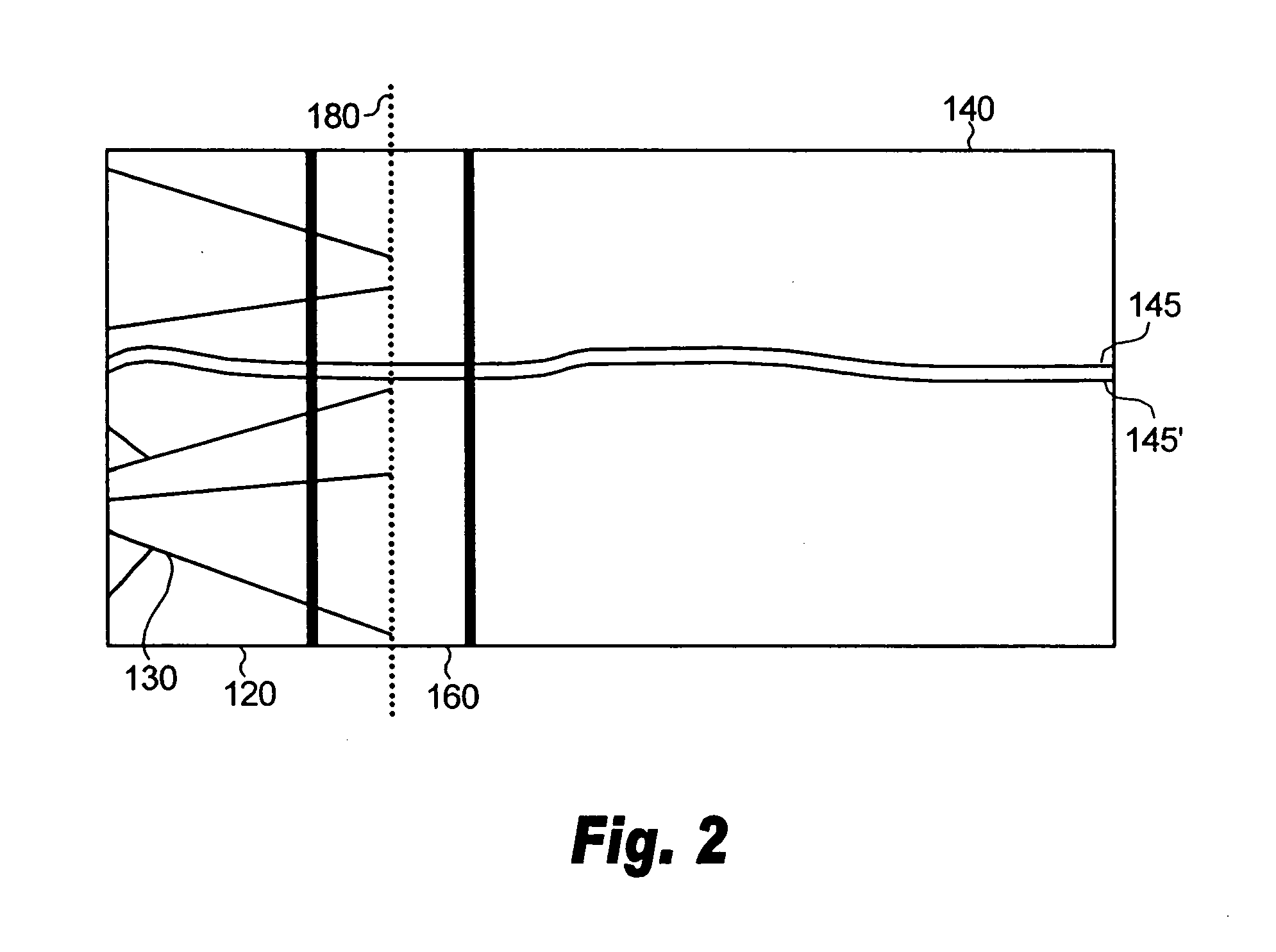
[0051] The crystallization of a thin film using a pulsed, narrow, elongated laser beam is described. The crystallization of a region of film following laser-induced melting is related to the characteristics of the laser pulse. In particular, the quality, size and shape of crystal grains in a crystallized region are determined by the energy, the spatial profile, and / or the temporal profile of the laser pulses that melt the region. Various irradiation schemes are described for polycrystalline substrates for use in display devices.

[0052] Pulse non-uniformities in an SLS system used to produce crystalline semiconductor films can arise from non-uniformities within a given laser pulse, as well as variations between successive pulses. For example, within a given laser pulse, the spatial energy density profile (e.g., uniformity of irradiation), the temporal intensity profile (e.g., pulse duration and / or temporal shape), and / or the imaging (e.g., field curvature and distortion) may vary. In...


PUM

PropertyMeasurementUnit
angleaaaaaaaaaa
angleaaaaaaaaaa
width aspect ratioaaaaaaaaaa

Abstract

A polycrystalline film is prepared by (a) providing a substrate having a thin film disposed thereon, said film capable of laser-induced melting, (b) generating a sequence of laser pulses having a fluence that is sufficient to melt the film throughout its thickness in an irradiated region, each pulse forming a line beam having a predetermined length and width, said width sufficient to prevent nucleation of solids in a portion of the thin film that is irradiated by the laser pulse, (c) irradiating a first region of the film with a first laser pulse to form a first molten zone, said first molten zone demonstrating a variation in width along its length to thereby define a maximum width (Wmax) and a minimum width (Wmin), wherein the first molten zone crystallizes upon cooling to form one or more laterally grown crystals, (d) laterally moving the film in the direction of lateral growth a distance that is greater than about one-half Wmax and less than Wmin; and (e) irradiating a second region of the film with a second laser pulse to form a second molten zone having a shape that is substantially the same as the shape of the first molten zone, wherein the second molten zone crystallizes upon cooling to form one or more laterally grown crystals that are elongations of the one or more crystals in the first region.

Description

CROSS REFERENCE TO RELATED APPLICATION [0001] This application claims the benefit under 35 U.S.C. §119(e) of U.S. Provisional Patent Application No. 60 / 668,934, filed on Apr. 6, 2005, entitled Line Scan Sequential Lateral Solidification of Thin Films, which is herein incorporated by reference in its entirety.FIELD OF THE INVENTION [0002] This invention relates to processing for thin film materials, and more particularly to forming crystalline thin films from amorphous or polycrystalline thin films using a line beam laser irradiation. In particular, the present disclosure relates to systems and methods for processing thin films to obtain substantial performance uniformity of thin film transistors (“TFTs”) situated therein. BACKGROUND OF THE INVENTION [0003] In recent years, various techniques for crystallizing or improving the crystallinity of an amorphous or polycrystalline semiconductor film have been investigated. This technology is used in the manufacture of a variety of devices,...

Claims


Application Information

Patent Timeline
Patent Type & Authority Applications(United States)
IPC IPC(8): C30B21/04C30B13/00C30B28/08
CPCB23K26/0738C30B13/00C30B13/24C30B29/06Y10T117/1008H01L27/1285H01L27/1296Y10T117/10Y10T117/1004H01L21/2026H01L21/02532H01L21/02678H01L21/02686H01L21/02691C30B21/04C30B28/08
Inventor IM, JAMES S.VAN DER WILT, PAUL C.
Owner THE TRUSTEES OF COLUMBIA UNIV IN THE CITY OF NEW YORK
Why Eureka
Try Eureka