Post Dispersion Spatially Filtered Raman Spectrometer

a raman spectrometer and spatial filtering technology, applied in the field of raman spectrometers, can solve the problems of reducing the input power, the return on resolution the rapid decline of the pixel size, so as to reduce the size and cost of the detector

Inactive Publication Date: 2006-11-16
AXSUN TECH
View PDF1 Cites 11 Cited by
  • Summary
  • Abstract
  • Description
  • Claims
  • Application Information

AI Technical Summary

Benefits of technology

[0010] The present invention seeks to further reduce the size and cost of the detector, and the spectrometer, by removing the restriction of discrete orders physically spaced from one another.

Problems solved by technology

Decreasing the pixel size further has rapidly diminishing returns on resolution.
In the case of reducing the entrance slit, input power is reduced, which is undesirable for a Raman spectrometer that is typically light starved.

Method used


Image

  • Post Dispersion Spatially Filtered Raman Spectrometer
  • Post Dispersion Spatially Filtered Raman Spectrometer
  • Post Dispersion Spatially Filtered Raman Spectrometer

Examples


second embodiment

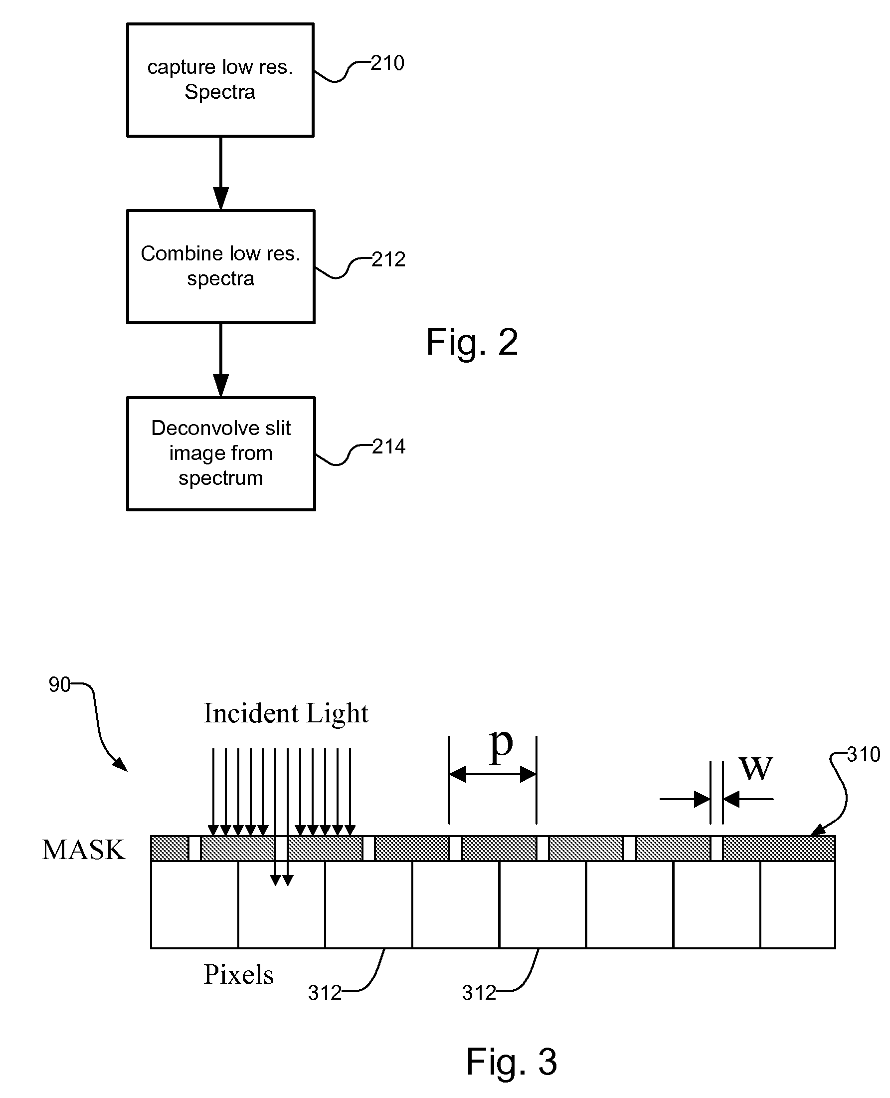
[0043]FIG. 3 illustrates a configuration of the detector array 90 used in the present invention. This embodiment avoids the need to perform the deconvolution step.

[0044] The second embodiment achieves the effective resolution by masking the detector array 90 itself using a physical aperture mask 310. The aperture mask has the same pitch, p, as the detector elements 312 but the transmission width, w, is equal to the desired effective pixel size.

[0045] The pattern, or mask, 310 is preferably aligned precisely during the fabrication of the detector array 90. The transmission width is roughly centered on a pixel of the array. In this way, each detector pixel 312 responds to light from one and only one mask window whose width is the desired effective pixel size. This eliminates detector pixel crosstalk and if the mask is made by photolithographic techniques, it will approximate an ideal rectangle sampling function.

[0046] Then, the multiple spectra sampled with this mask 310 are prefera...

first embodiment

[0048] As in the first embodiment, deconvolution with the entrance slit image can be performed if required provided the Nyquist sampling is satisfied and the optics are sufficiently flat field. Alternatively, if the input slit is sufficiently narrow, no deconvolution is required, provided the mask can be fabricated with sufficiently narrow slit width w to achieve the desired resolution. This allows the minimum detector area to be realized, i.e., that for which the spectral resolution element is no larger than the smallest required to achieve the target SNR requirement. The penalty for this small size is that the mask only allows a small fraction of the incident light to strike a detector pixel. Due to the convolution of the spectrum with the image of the entrance slit, this corresponds to an extra insertion loss. The magnitude of the loss is estimated as IL=10*log(w / (Slit Image)).

[0049] For either embodiment, the total spectrum shift required in the low-resolution images is equal to...


PUM

PropertyMeasurementUnit
Ramanaaaaaaaaaa
Raman spectraaaaaaaaaaa
wavelengthaaaaaaaaaa

Abstract

To achieve a given spectral resolution with reduced detector size and commercially available pixel pitches, the Raman spectrum is shifted across the detector array such as by one of the following methods: 1) tuning the excitation wavelength; 2) rotating the grating; 3) displacing the effective input slit (fiber) and acquiring the spectrum under stepped displacement conditions; and 4) displacement of a lens relative to input fiber to displace effective input slit relative to the detector. A composite spectrum is formed and deconvolution of the entrance aperture image and/or pixel masking is then used.

Description

RELATED APPLICATIONS [0001] This claims the benefit of U.S. Provisional Application No. 60 / 680,878, filed May 13, 2005, which is incorporated herein by reference in its entirety.BACKGROUND OF THE INVENTION [0002] Conventional Raman spectrometers use a fixed wavelength laser source and a notch filter on the return path to block the source wavelength but allow the Stokes-shifted wavelengths to pass. A dispersive element is used to then to spatially disperse the Raman response. A multi-element detector is used to detect the dispersed Raman spectra. The size of detector is selected so that it provides enough elements (pixels) such that each pixel provides one wavelength resolution element. [0003] In these conventional systems, resolution is generally limited by the entrance slit as it is imaged onto the detector and thus convolves the spectrum. The physical size of the detector's active area and the spatial dispersion (product of angular dispersion and lens focal length) set the range o...

Claims


Application Information

Patent Timeline
Patent Type & Authority Applications(United States)
IPC IPC(8): G01J3/44G01N21/65
CPCG01J3/02G01N2021/399G01J3/0227G01J3/0229G01J3/0237G01J3/04G01J3/06G01J3/10G01J3/28G01J3/44G01J2003/065G01N21/39G01N21/65G01N2021/1772G01J3/0218
Inventor COPPETA, DAVID A.
Owner AXSUN TECH
Why Eureka
Try Eureka