
Method of repairing disconnection, method of manufacturing active matrix substrate by using thereof, and display device

a technology of active matrix substrate and disconnection, which is applied in the direction of semiconductor devices, instruments, electrical equipment, etc., can solve the problems of increasing stress, reducing the adhesion of film, and affecting so as to reduce the display defect of the display device, improve the yield of wiring repair, and enhance the adhesion of conductive film

Inactive Publication Date: 2006-11-16
NEC LCD TECH CORP
View PDF11 Cites 1 Cited by
  • Summary
  • Abstract
  • Description
  • Claims
  • Application Information

AI Technical Summary

Benefits of technology

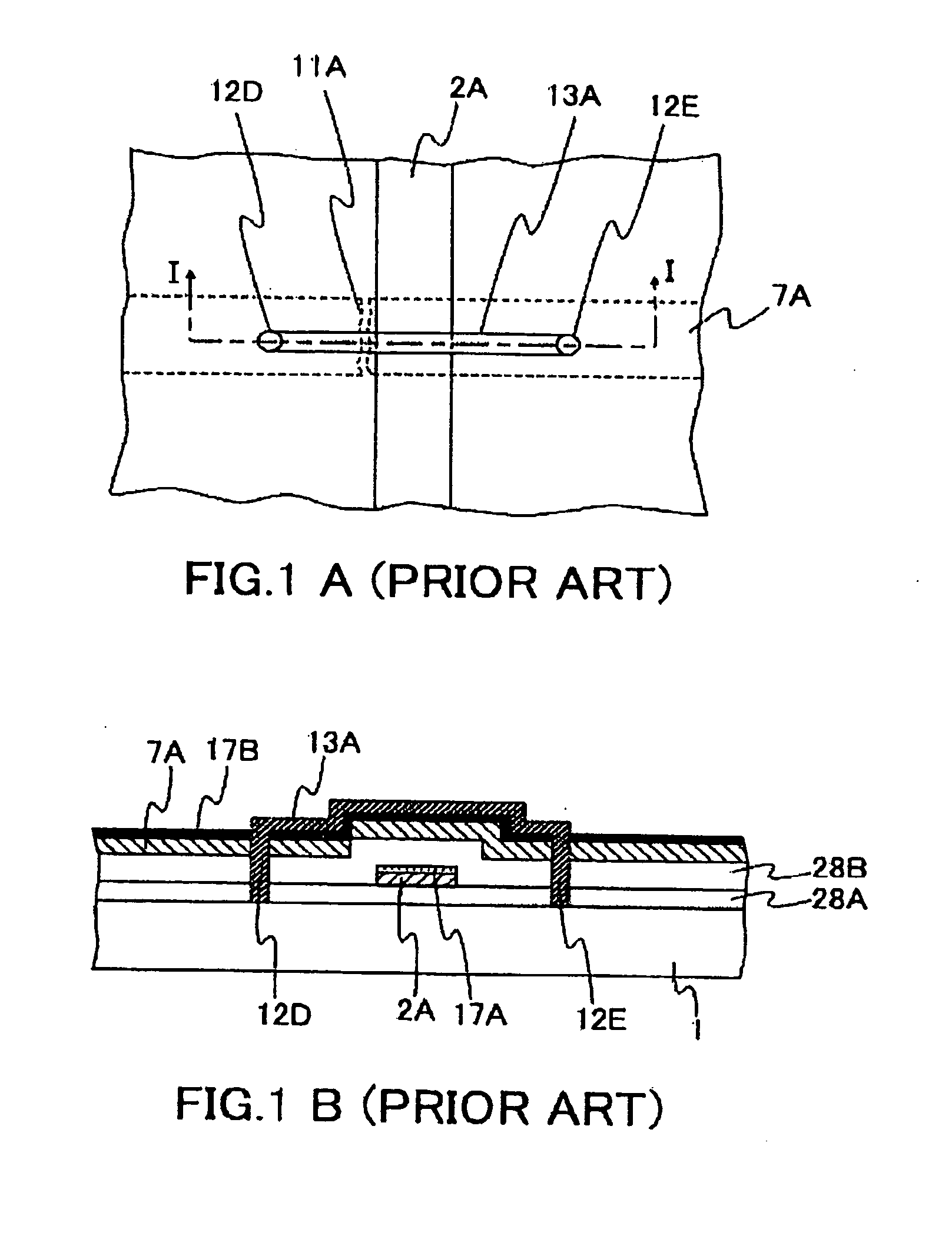
[0010] With the aforementioned problems taken into consideration, the present invention has been made. The present invention provides a disconnection repairing method using a laser CVD method which controls generating of a leak current among a part where a disconnected wiring has been repaired and each of pixel electrodes and another wiring, or parasitic capacitance, and can reduce a display defect on a display device. The present invention provides a method of manufacturing an active matrix substrate, and a display device including the active matrix substrate, using the disconnection repairing method.
[0011] Furthermore, in the case where a disconnected wiring on a display device is repaired by use of the laser CVD method, the present invention provides a disconnection repairing method, a method of manufacturing an active matrix substrate, and a display device including the active matrix substrate, whereby the adhesion of the repaired wiring to the underneath films is enhanced.

Problems solved by technology

In a TFT manufacturing process, if a conductor defect occurs due to a disconnection of a wiring, an active matrix display device, such as a liquid crystal display (LCD) device and an organic electroluminescence (EL) display device, becomes defective as well.
However, if the thickness of the conductive film to repair is too thick, this increases the stress, and accordingly decreases the adhesion of the film.
In addition, if the width of the film to repair wiring is formed wider, this causes a leak current between the repaired wiring and the pixel electrode.
However, even in a case where a part of disconnection of the wiring is repaired with these conditions, the repair causes a leak current between the repaired wiring and the pixel electrode.
Accordingly, this brings about a problem of causing a leak current between the repaired wiring and the pixel electrode.
As a result, this brings about a problem of causing a display defect, because the pixel electrode cannot hold proper voltage, that is, data retention characteristics is degraded.
However, even in this case, when the disconnected wiring is repaired by the laser CVD method, conductive fine particles formed by laser CVD remain in a vicinity of the part where the wiring has been repaired.
Since an area where these conductive fine particles formed by laser CVD are condense and connected is conductive, additional parasitic capacity is caused between the pixel electrode and the part where the disconnected wiring has been repaired.
Accordingly, this brings about a problem of causing a display defect, because the pixel electrode voltage is influenced by the repaired data signal wiring.

Method used


Image

  • Method of repairing disconnection, method of manufacturing active matrix substrate by using thereof, and display device
  • Method of repairing disconnection, method of manufacturing active matrix substrate by using thereof, and display device
  • Method of repairing disconnection, method of manufacturing active matrix substrate by using thereof, and display device

Examples


first example

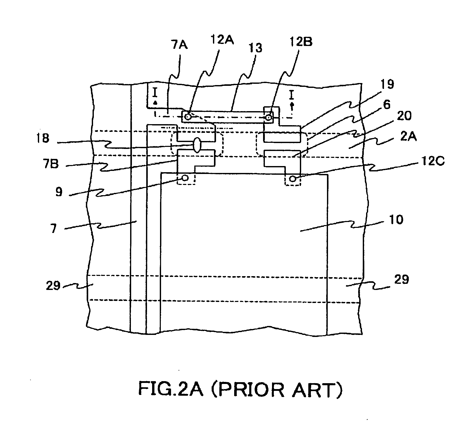
[0046] Descriptions will be provided for a method of manufacturing an active matrix substrate and a display device including the active matrix substrate according to the first example of the present invention with reference to FIGS. 3, 4, 5A to 5C, and 6A to 6D.

[0047] First of all, by use of the foregoing method of manufacturing an active matrix liquid crystal display device, pixel electrodes 10 of a TFT substrate are formed. After that, it is inspected whether or not each of the wirings is disconnected. In a case where a predetermined wiring (a data signal wiring 7 in this example) is disconnected, a defective part 11 of disconnection is located (see FIG. 6A). Subsequently, pulsed Nd: YLF (Neodymium:yttrium lithium fluoride) laser with a wavelength of 351 nm is irradiated thereon. Thereby, contact holes 12A and 12B for repair are made in the passivation film 8 at the two ends of the defective part 11 of disconnection as shown in FIG. 6B. Thereafter, by use of a film-forming gas ma...

second example

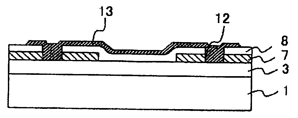
[0053] Descriptions will be provided for a method of manufacturing an active matrix substrate (TFT substrate) and a display device including the active matrix substrate according to a second example of the present invention with reference to FIGS. 7, 8A to 8C, and 9A to 9C.

[0054] In the case of the first example, a disconnection of a data signal wiring 7 is repaired after forming the pixel electrodes 10. In the case of the second example, a disconnection of a data signal wiring 7 is repaired after forming the data signal wiring 7, and before forming a passivation film 8.

[0055] First of all, the inspection is made after the data signal wiring 7 is formed. In a case where the data signal wiring 7 is disconnected, a defective part 11 of disconnection is located (see FIG. 9A). Subsequently, as shown in FIGS. 7, 8A and 9B, a conductive film 13 is selectively formed in the defective part 11 of disconnection by the laser CVD method. Thereafter, as shown in FIGS. 7 and 8B, laser is irradi...

third example

[0058] Hereinafter, descriptions will be provided for a method of manufacturing an active matrix substrate (TFT substrate) and a display device including the active matrix substrate according to a third example of the present invention with reference to FIG. 10.

[0059] In the case of the first example, the laser is irradiated on the region between the conductive film 13 and each of the pixel electrodes 10 without damaging the conductive film 13, the data signal wiring 7 and the pixel electrode 10. By reducing the power of the laser, conductive fine particles 14A on a surrounding area 14 of a conductive film 13 can be removed therefrom while inhibiting the conductive film 13, a data signal wiring 7 and a pixel electrode 10 from being damaged.

[0060] For example, as shown in FIG. 10, a Nd: YLF laser is irradiated in a scanning manner on an area 15 for laser light irradiation, inclusive of the conductive film 13 which has been selectively formed, in conditions of a 3% laser transmittan...


PUM


Abstract

A part where a wiring is disconnected is repaired by the laser CVD method while active matrix substrates for liquid crystal display devices and organic electroluminescence display devices are being manufactured. By the laser CVD method, a conductive film is selectively formed in the part where the wiring is disconnected. Thereafter, laser light is irradiated on at least a surrounding area of the conductive film, and thus conductive fine particles remaining in the surrounding area of the conductive film are removed therefrom. As a result, a leak current and parasitic capacity can be inhibited from occurring between the part where the disconnection has been repaired and another wiring.

Description

BACKGROUND OF THE INVENTION [0001] 1. Field of the Invention [0002] The present invention relates to a method of repairing disconnections of wirings formed on a substrate. Particularly, the present invention relates to a method of manufacturing an active matrix substrate using the method of repairing disconnections, and to a display device including the same. [0003] 2. Descriptions of the Prior Art [0004] Liquid crystal display devices having thin film transistors (hereinafter referred to as “TFTs”) as switching elements have been widely used. Amorphous silicon (hereinafter referred to as “a-Si”) is chiefly used for semiconductor films of TFTs. In addition, liquid crystal display devices using polycrystalline silicon for semiconductor films of TFTs have been commercialized. Furthermore, organic electroluminescence display devices in which pixel circuits comprise with polycrystalline silicon TFTs have been developed. [0005] In a TFT manufacturing process, if a conductor defect occurs...

Claims


Application Information

Patent Timeline
Patent Type & Authority Applications(United States)
IPC IPC(8): H01L21/00
CPCG02F1/136259H01L27/124G02F1/136286
Inventor OOISHI, MITSUMA
Owner NEC LCD TECH CORP
Learn More