Tunneling field effect transistor using angled implants for forming asymmetric source/drain regions

a tunneling field effect and angled implant technology, applied in the field of semiconductor manufacturing, can solve the problems of limiting the prior tfet fabrication of asymmetric processing, adversely increasing the transistor gate delay, and limiting the device to a single channel length

Inactive Publication Date: 2006-11-16
INTEL CORP
View PDF10 Cites 118 Cited by
  • Summary
  • Abstract
  • Description
  • Claims
  • Application Information

AI Technical Summary

Problems solved by technology

Asymmetric processing has limited the prior TFET fabrication attempts to vertical growth of the source, channel, and drain regions, requiring a side gate oxide and gate electrode deposition.
This process suffers from high overlap capacitance between the gate and source / drain regions which adversely increases the transistor gate delay and limits the device to a single channel length.
The TFET also suffers from high gate leakage due to the oppositely biased source and gate nodes.

Method used


Image

  • Tunneling field effect transistor using angled implants for forming asymmetric source/drain regions
  • Tunneling field effect transistor using angled implants for forming asymmetric source/drain regions
  • Tunneling field effect transistor using angled implants for forming asymmetric source/drain regions

Examples


Embodiment Construction

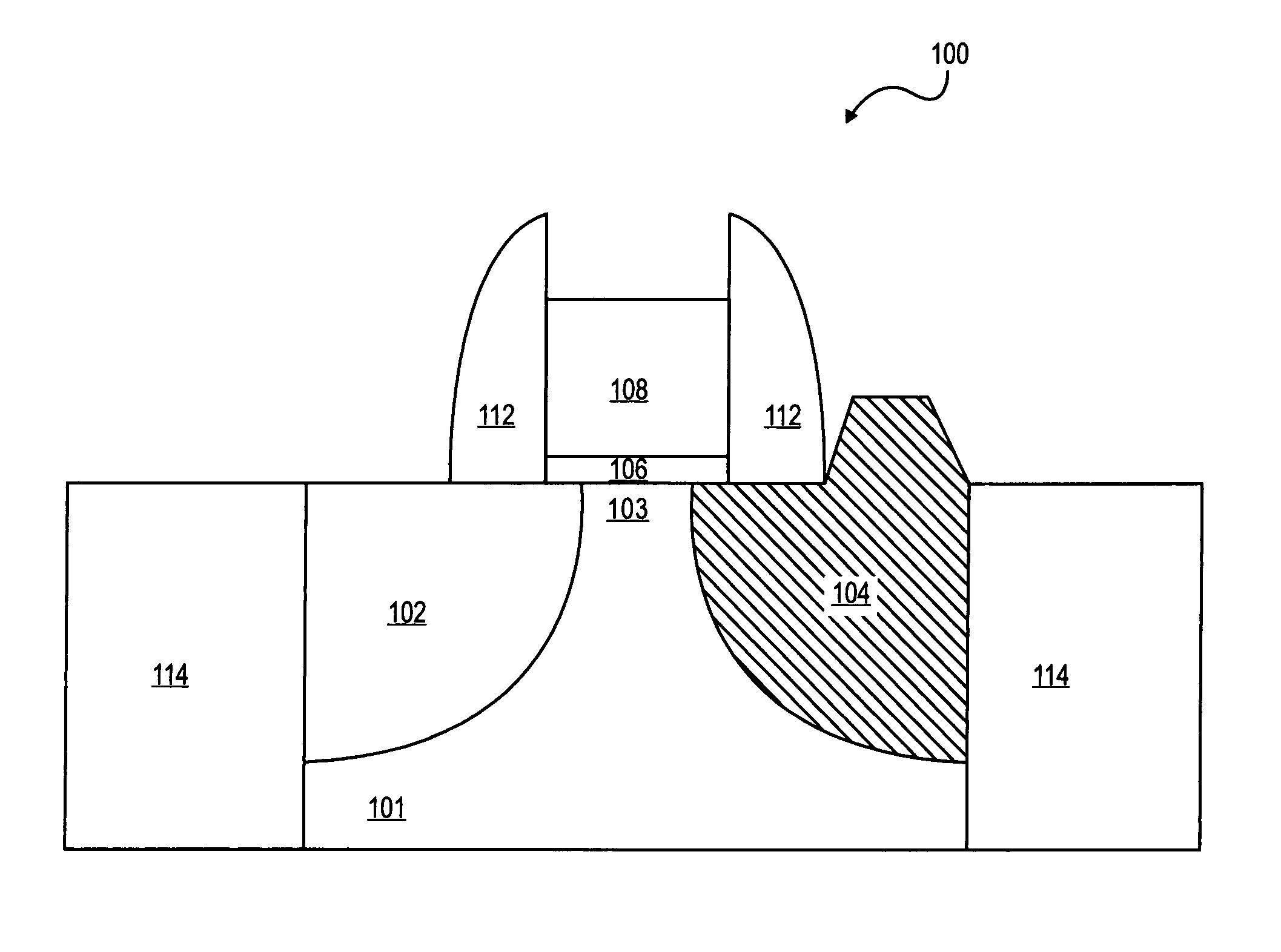
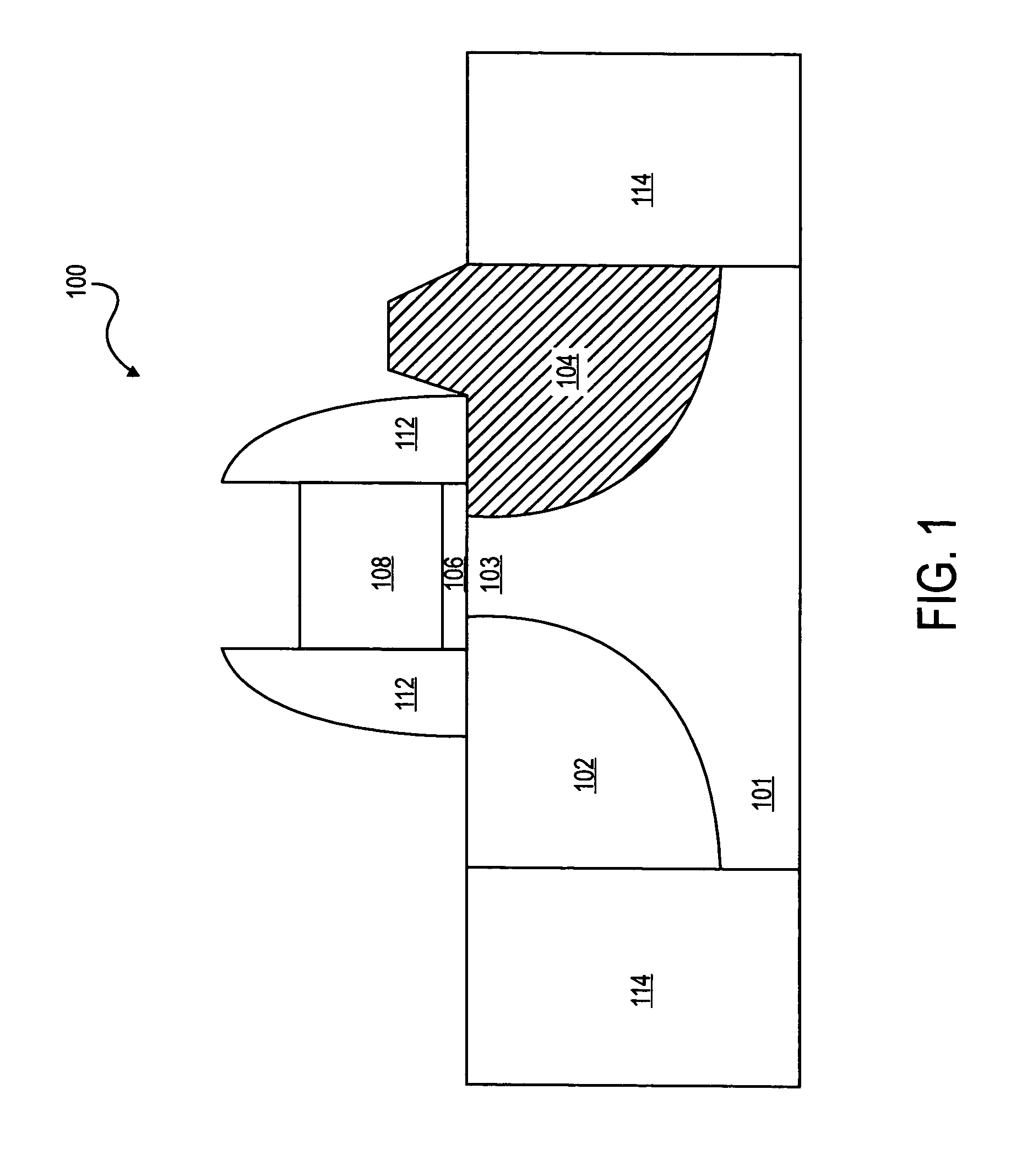
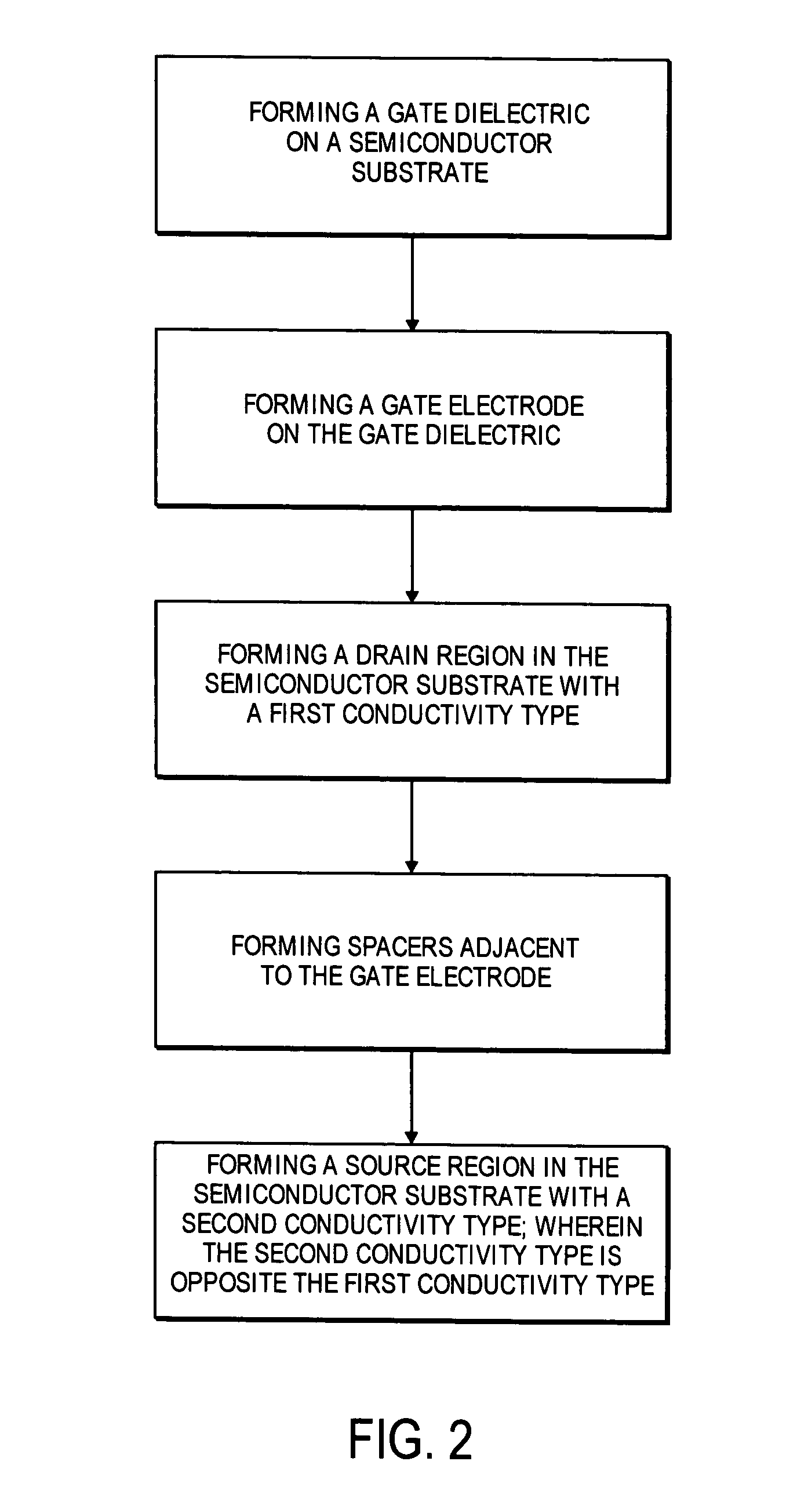
[0011] In an embodiment, the present invention includes a planar Tunneling Field Effect Transistor (TFET) comprising asymmetric transistor terminals, an epitaxial grown source region, and multiple transistor gate lengths. In an embodiment, the planar TFET is n-type, which features a p-type silicon germanium alloy epitaxial source region and a silicon drain region with an N+ type conductivity. The planar TFET of the present invention may be manufactured p-type. In an embodiment, this asymmetry is achieved by a shadowing technique provided by both a properly-size, patterned gate stack and angled implants. Planar TFET's are advantageous because short channel effects, such as drain induced barrier lowering (DIBL) and sub-threshold swing (ΔS), caused by progressive gate length scaling, are improved without performance limiters attributable to vertical TFET's. To increase performance, an embodiment utilizes a high-k gate dielectric to remedy the effect of gate tunneling leakage due to dua...


PUM


Abstract

The present invention relates to a Tunnel Field Effect Transistor (TFET), which utilizes angle implantation and amorphization to form asymmetric source and drain regions. The TFET further comprises a silicon germanium alloy epitaxial source region with a conductivity opposite that of the drain.

Description

BACKGROUND [0001] 1. Field [0002] The present invention relates to the field of semiconductor manufacturing, specifically a planar Tunneling Field Effect Transistor (TFET) which features asymmetric source / drain terminals and a silicon germanium alloy epitaxial source region. [0003] 2. Description of Related Art [0004] As MOSFET gate length scaling continues, controlling short channel effects such as drain induced barrier lowering and sub-threshold swing is imperative for improved performance. Tunnel Field Effect Transistors (TFET's) can improve both of these parameters by changing the injection mechanism and provide asymmetric doping to the source and drain regions of the device. Asymmetric processing has limited the prior TFET fabrication attempts to vertical growth of the source, channel, and drain regions, requiring a side gate oxide and gate electrode deposition. This process suffers from high overlap capacitance between the gate and source / drain regions which adversely increase...

Claims


Application Information

Patent Timeline
Patent Type & Authority Applications(United States)
IPC IPC(8): H01L21/8234
CPCH01L29/7391
Inventor KAVALIEROS, JACK T.METZ, MATTHEW V.DEWEY, GILBERTJIN, BEEN-YIHBRASK, JUSTIN K.DATTA, SUMANCHAU, ROBERT S.
Owner INTEL CORP
Why Eureka
Try Eureka