Semiconductor device

Inactive Publication Date: 2006-11-23
SEMICON ENERGY LAB CO LTD
View PDF65 Cites 58 Cited by
  • Summary
  • Abstract
  • Description
  • Claims
  • Application Information

AI Technical Summary

Benefits of technology

[0021] By applying the present invention, it is possible to write (additionally record) data at a time other than during manufacturing a chip but impossible to rewrite the data. Therefore, a semiconductor device capable of preventing forgery due to rewriting can be obtained. Moreover, since a semiconductor device of the present invention has a storage element with a simple structure in which an organic compound layer is sandwiched between a pair of conductive layers, the semiconductor device can be inexpensive. Furthermore, since writing is carried out in a semicond

Problems solved by technology

Although a mask ROM has a simple structure, data need to be written

Method used


Image

  • Semiconductor device
  • Semiconductor device
  • Semiconductor device

Examples


embodiment modes

[0038] Embodiment modes and embodiments of the present invention will be described with reference to the drawings. However, it is easily understood by those skilled in the art that the mode and detail can be variously modified without departing from the scope and spirit of the present invention. Therefore, the present invention is not construed as being limited to the description of embodiment modes and embodiments. It is to be noted that reference numeral indicating the same part is used in common in different drawings in the structures of the present invention hereinafter described.

embodiment mode 1

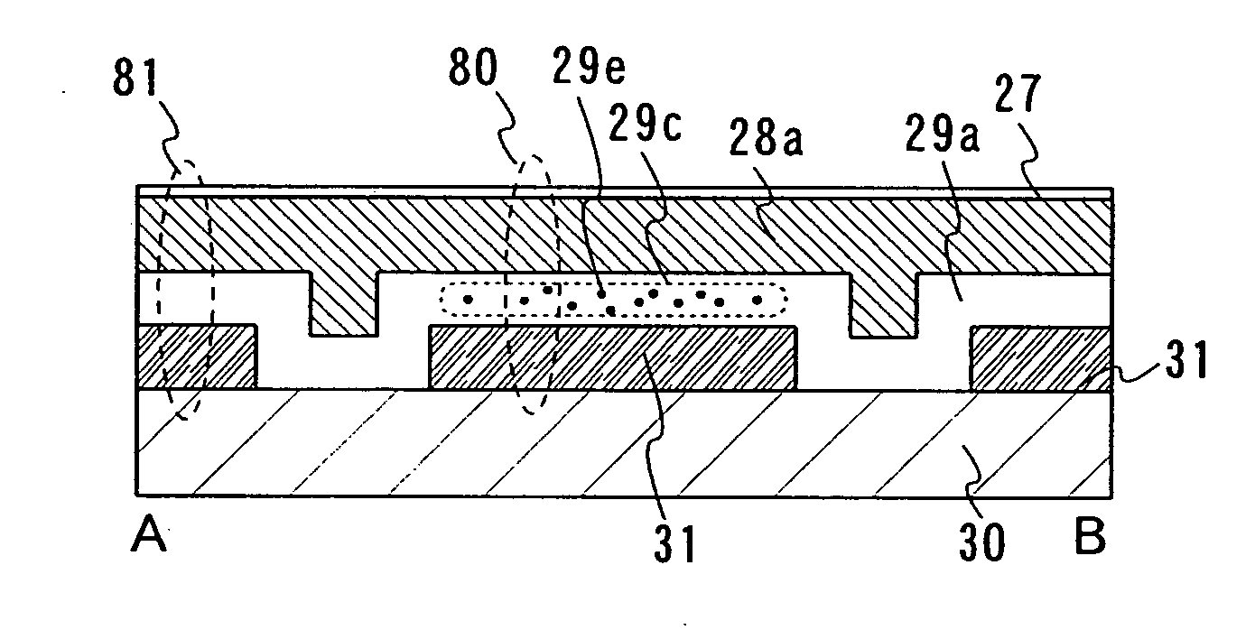
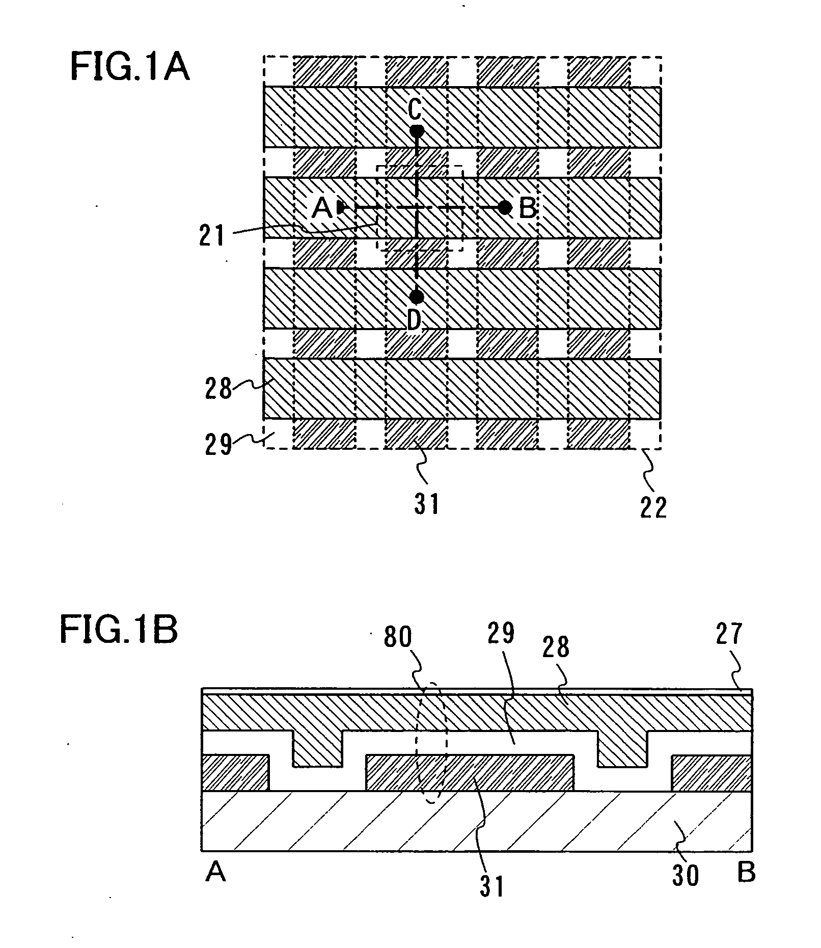
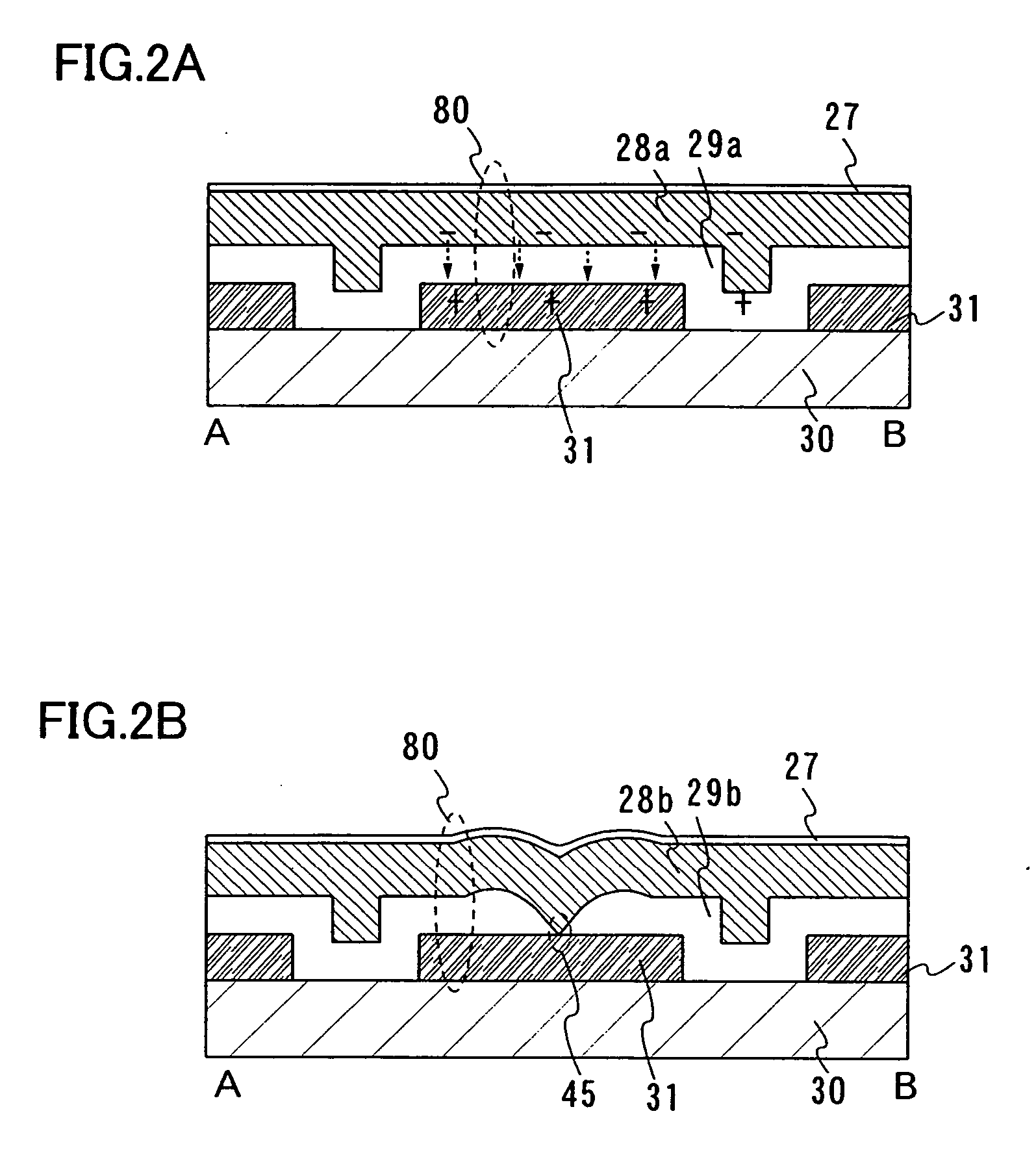
[0039] Embodiment Mode 1 will describe a structural example of a storage element in a semiconductor device of the present invention with reference to the drawings. More specifically, a case of a passive matrix semiconductor device is shown.

[0040]FIG. 5A shows a structural example of a storage element of this embodiment mode, which includes a memory cell array 22 in which memory cells 21 are arranged in matrix; a bit line driver circuit 26 having a column decoder 26a, a reading / writing circuit 26b, and a selector 26c; a word line driver circuit 24 having a row decoder 24a and a level shifter 24b; and an interface 23 having a writing circuit and the like, that communicates with outside. The structure of the storage circuit 16 shown here is just an example and the storage circuit 16 may have other circuits such as a sense amplifier, an output circuit, and a buffer, and the writing circuit may be provided in the bit line driver circuit.

[0041] The memory cell 21 has a first conductive ...

embodiment mode 2

[0088] Embodiment Mode 2 will describe a semiconductor device having a structure which is different from that shown in Embodiment Mode 1. Specifically, a case of an active matrix semiconductor device will be shown.

[0089]FIG. 6A shows a structural example of a semiconductor device described in Embodiment Mode 2. A memory cell array 222 in which memory cells 221 are arranged in matrix; a bit line driver circuit 226 including a column decoder 226a, a reading / writing circuit 226b, and a selector 226c; a word line driver circuit 224 including a row decoder 224a and a level shifter 224b; and an interface 223 including a writing circuit and the like, which communicates with outside are provided. The structure of a storage circuit 216 shown here is just an example and the storage circuit 216 may further include other circuits, such as a sense amplifier, an output circuit, and a buffer, and the writing circuit may be provided in the bit line driver circuit.

[0090] The memory cell 221 has a ...


PUM


Abstract

It is an object of the present invention to provide a semiconductor device capable of additionally recording data at a time other than during manufacturing and preventing forgery due to rewriting and the like. Moreover, another object of the present invention is to provide an inexpensive, nonvolatile, and highly-reliable semiconductor device. A semiconductor device includes a first conductive layer, a second conductive layer, and an organic compound layer between the first conductive layer and the second conductive layer, wherein the organic compound layer can have the first conductive layer and the second conductive layer come into contact with each other when Coulomb force generated by applying potential to one or both of the first conductive layer and the second conductive layer is at or over a certain level.

Description

BACKGROUND OF THE INVENTION [0001] 1. Field of Invention [0002] The present invention relates to a semiconductor device provided with a storage element. [0003] 2. Description of the Related Art [0004] In recent years, development has been advanced on a semiconductor device having various functions in which a plurality of circuits are integrated over an insulating surface. Further, development has been advanced on a semiconductor device which can send and receive data wirelessly by providing an antenna. Such a semiconductor device is referred to as a wireless chip (also referred to as an ID tag, an IC tag, an IC chip, an RF (Radio Frequency) tag, a wireless tag, an electronic tag, or an RFID (Radio Frequency Identification) tag), and has already been introduced into some markets [0005] Many of semiconductor devices that are currently in practical use have circuits using semiconductor substrates such as Si (the circuits are also referred to as ICs (Integrated Circuits)) and antennas, ...

Claims


Application Information

Patent Timeline
IPC IPC(8): H01L29/08H01L29/04
CPCH01L23/5252H01L27/10H01L2224/73204Y10S257/908H01L2924/07811Y10S257/906H01L2924/00H01L2924/12044
Inventor YUKAWA, MIKIO
Owner SEMICON ENERGY LAB CO LTD
Why Eureka
Try Eureka