

Pixels for CMOS image sensors
- Summary
- Abstract
- Description
- Claims
- Application Information
AI Technical Summary
Benefits of technology
Problems solved by technology
Method used
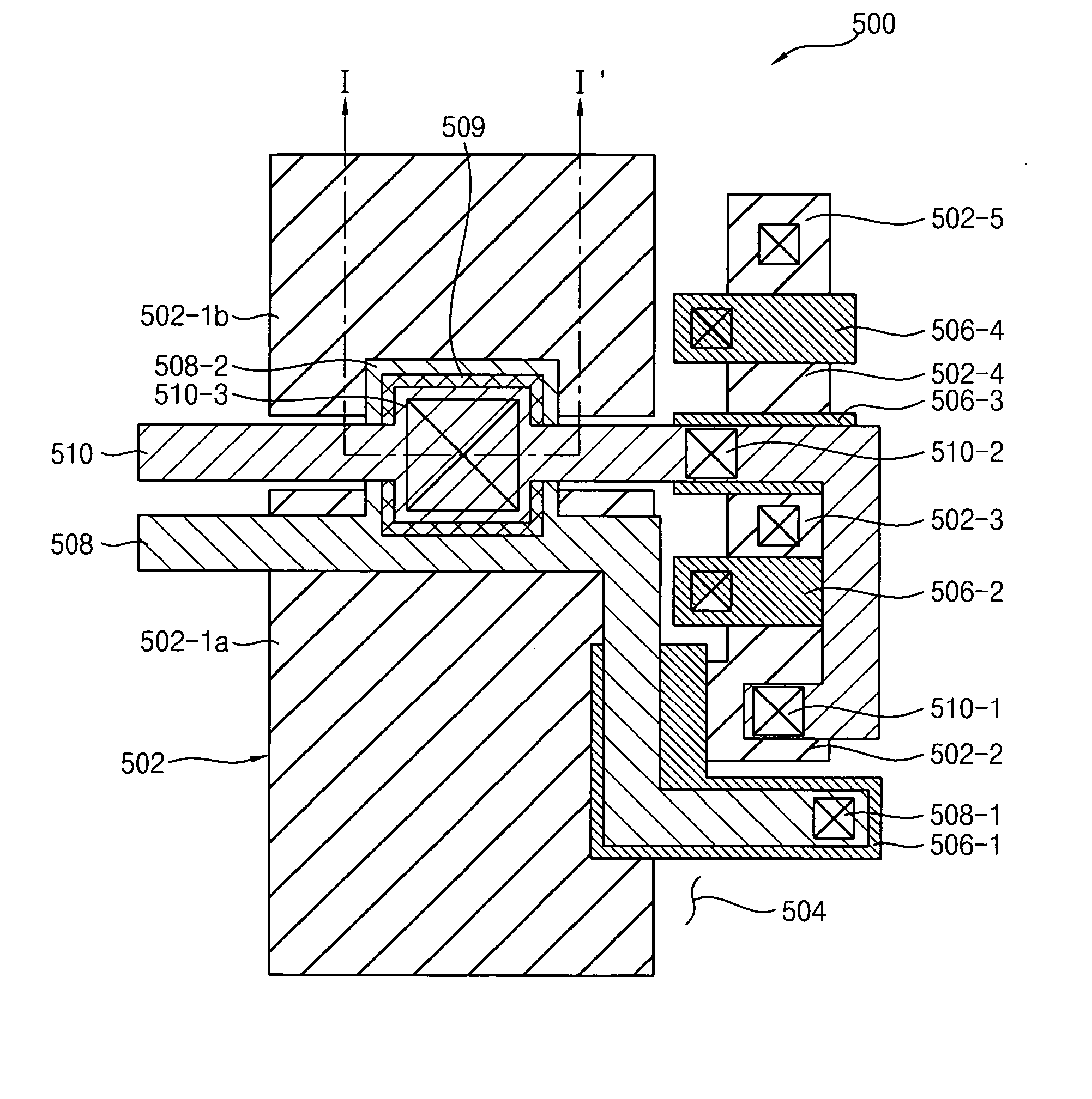
Image

Examples
Embodiment Construction
[0040] Exemplary embodiments of the present disclosure are disclosed herein. The specific structural and functional details shown are merely representative for purposes of describing the exemplary embodiments. Thus, the present invention may be embodied in many alternate forms and should not be construed as limited to the exemplary embodiments set forth herein.
[0041] Accordingly, while the invention is susceptible to various modifications and alternative forms, specific embodiments thereof are shown by way of example in the drawings and are described in detail herein. It shall be understood, however, that there is no intent to limit the invention to the particular exemplary forms described, but on the contrary, the invention is to cover all modifications, equivalents, and alternatives falling within its spirit and scope. Like numbers may refer to like elements throughout the descriptions of the figures.
[0042] It shall also be understood that, although the terms first, second, etc....
PUM
 Abstract
Description
Claims
Application Information