
Trench isolation structure in a semiconductor device and method for fabricating the same

Inactive Publication Date: 2006-11-23
SK HYNIX INC
View PDF6 Cites 103 Cited by
  • Summary
  • Abstract
  • Description
  • Claims
  • Application Information

AI Technical Summary

Benefits of technology

[0010] The embodiments of the present invention to provide a trench isolation structure in a semiconductor device, in which the deposition of a liner oxide film is omitted and refresh characteristics are improved without deteriorating device characteristics at peripheral circuit regions.
[0011] Many benefits are achieved by way of the present invention over conventional techniques. For example, the present technique provides an easy to use process that relies upon conventional technology. In some embodiments, a trench isolation structure in a semiconductor device and a method for fabricating the same are provided in which the deposition of a liner oxide film is omitted and refresh characteristics are improved without deteriorating device characteristics at peripheral circuit regions. In some embodiments, the occurrence of hot electron induced punchthrough is reduced and a gapfill margin for the standard trench isolation region is increased. Additionally, the method provides a process that is compatible with conventional process technology without substantial modifications to conventional equipment and processes. Depending upon the specific embodiment, one or more of these benefits may be achieved. These and other benefits will be described in more throughout the present specification and more particularly below.

Problems solved by technology

However, the liner nitride film can also exert a negative influence on peripheral circuit regions.
Further, as described above, liner nitride film 150 promotes the trapping of hot electrons at the peripheral circuit regions, and thus increases the occurrence of HEIP in p-type MOS transistors, thereby causing deterioration of characteristics of the semiconductor device, such as reduction in the threshold voltage and increase in leakage current in an OFF state.

Method used


Image

  • Trench isolation structure in a semiconductor device and method for fabricating the same
  • Trench isolation structure in a semiconductor device and method for fabricating the same
  • Trench isolation structure in a semiconductor device and method for fabricating the same

Examples


Embodiment Construction

[0015] The present invention is directed to integrated circuits and their processing for the manufacture of semiconductor devices. More particularly, the invention provides a novel trench isolation structure and method used for electrical isolation in semiconductor devices. Merely by way of example, the invention has been applied to the manufacture of dynamic random access memory (DRAM). But it would be recognized that the invention has a much broader range of applicability. For example, the invention can be applied to microprocessor devices, logic circuits, application specific integrated circuit devices, as well as various other structures.

[0016] Now, a specific embodiment of the present invention will be described in detail with reference to the drawings. However, the present invention is not limited to this specific embodiment, and may have various other embodiments. In the drawings, certain elements are enlarged to clearly illustrate various layers and regions.
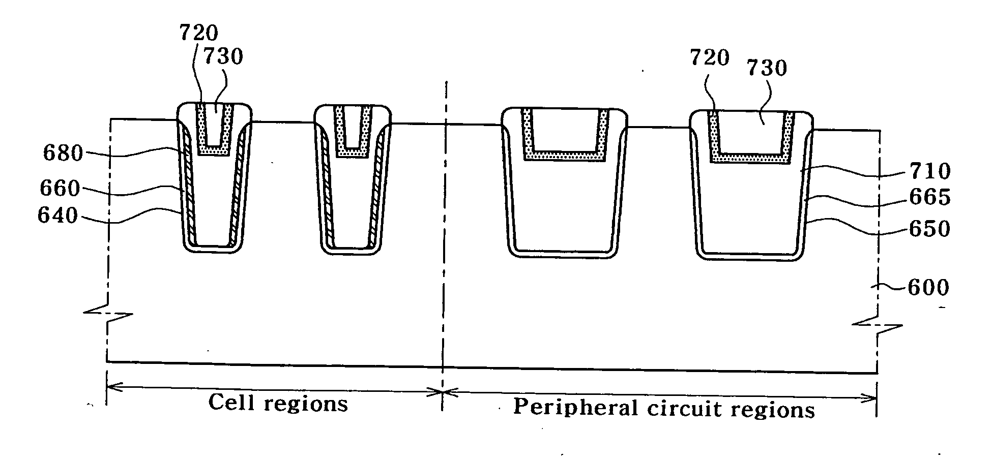
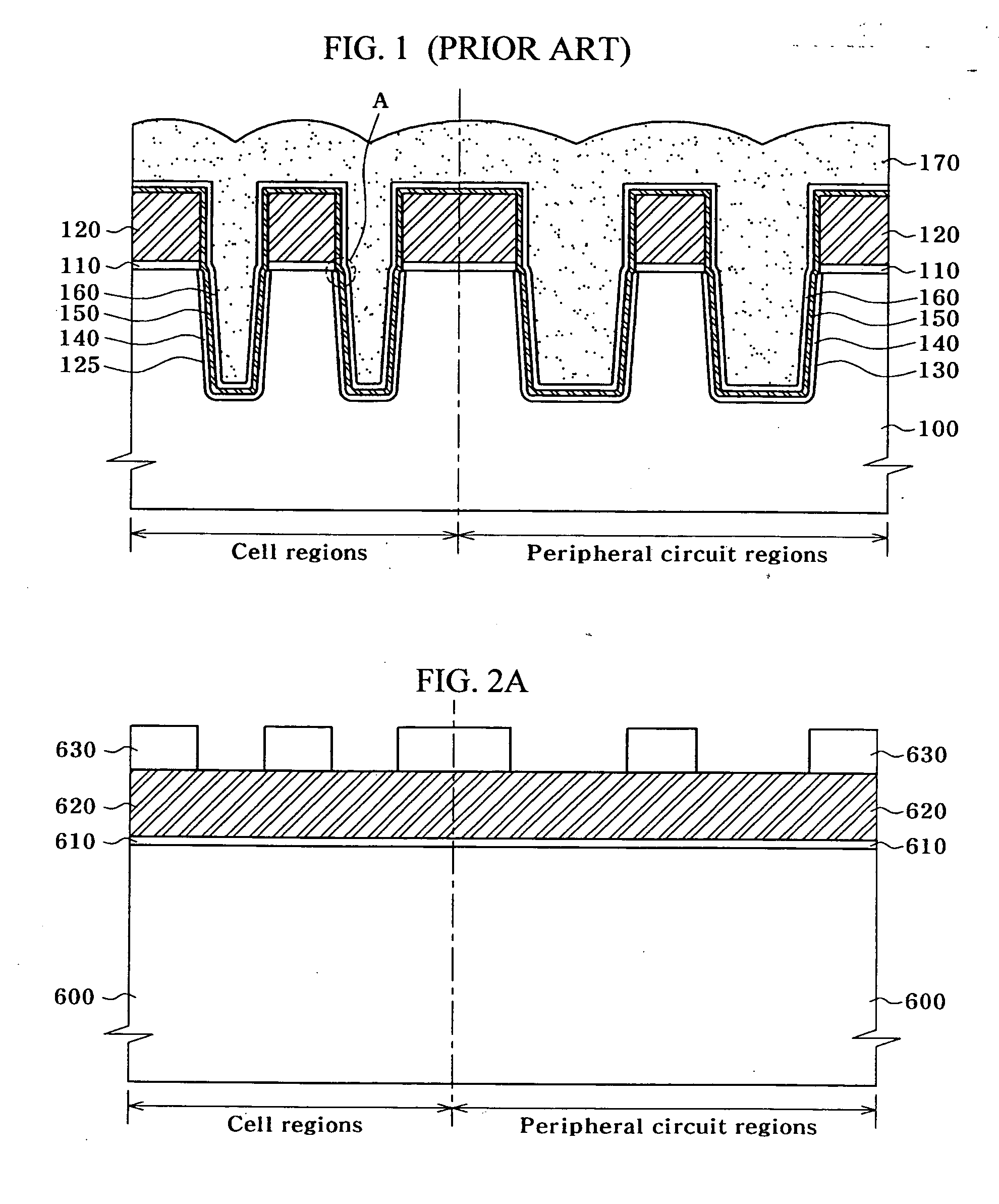
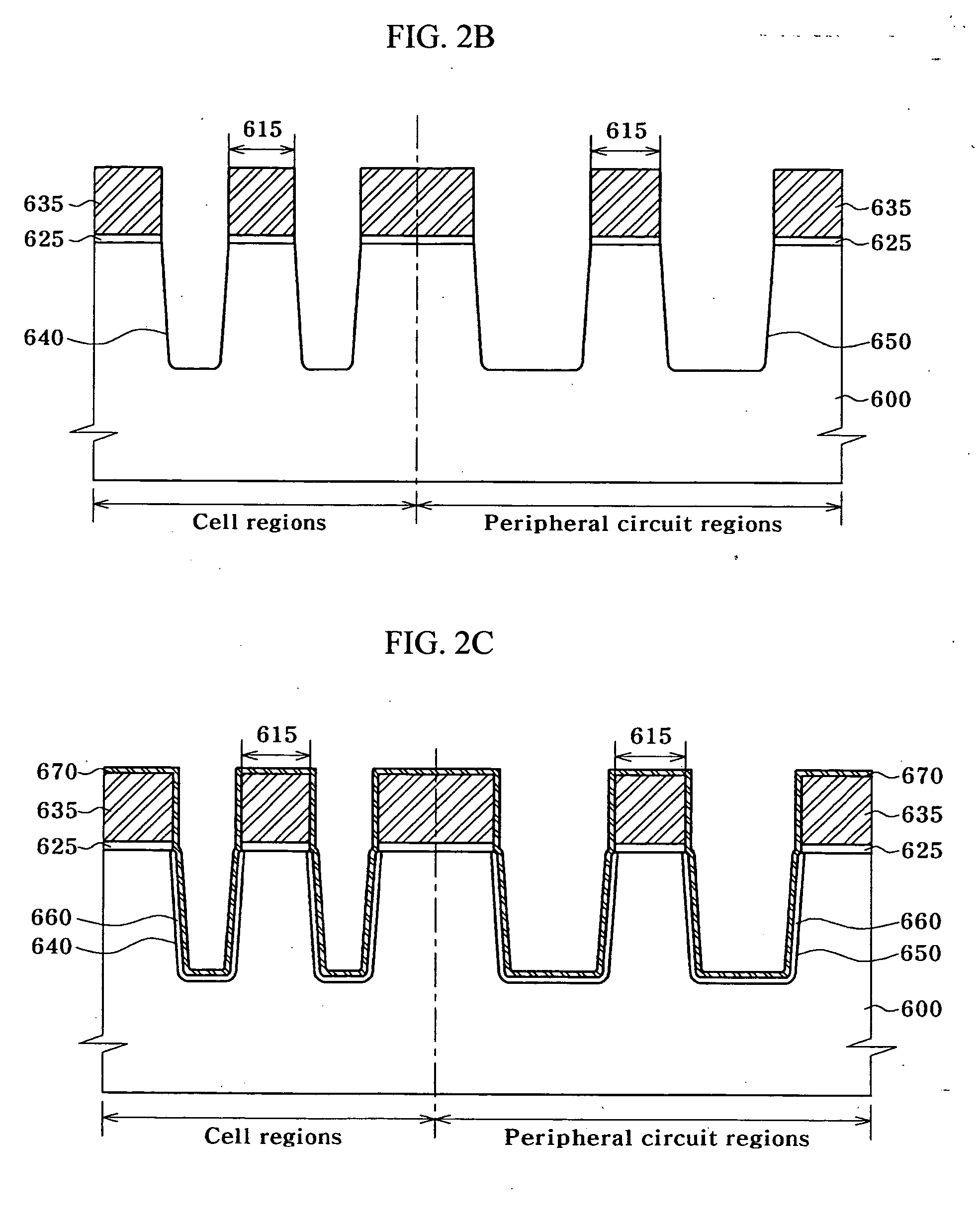
[0017]FIGS. 2A ...


PUM


Abstract

A trench isolation structure in a semiconductor device is provided. A semiconductor substrate has cell regions and peripheral circuit regions. First trenches have a predetermined depth and are formed in the semiconductor substrate at the cell regions. A first sidewall oxide film is formed overlying the first trenches. A first liner nitride film is formed overlying the first sidewall oxide film. Second trenches have a predetermined depth and are formed in the semiconductor substrate at the peripheral circuit regions. A second sidewall oxide film is formed overlying the second trenches. An oxide film fills the first overlying second trenches. A second liner nitride film formed on the filling oxide film. The second liner nitride film is separated from the sidewalls of the first and second trenches.

Description

BACKGROUND OF THE INVENTION [0001] The present invention is directed to integrated circuits and their processing for the manufacture of semiconductor devices. More particularly, the invention provides a novel trench isolation structure and method used for electrical isolation in semiconductor devices. Merely by way of example, the invention has been applied to the manufacture of dynamic random access memory (DRAM). But it would be recognized that the invention has a much broader range of applicability. For example, the invention can be applied to microprocessor devices, logic circuits, application specific integrated circuit devices, as well as various other structures. [0002] As semiconductor devices have become highly integrated, patterns have become finer and a process for fabricating a shallow trench isolation (hereinafter, referred to as “STI”) structure having small width and excellent isolation characteristics has become increasingly important. The trench isolation structure ...

Claims


Application Information

Patent Timeline
IPC IPC(8): H01L21/76
CPCH01L27/10894H01L21/76229H10B12/09H01L21/762
Inventor EUN, BYUNG SOO
Owner SK HYNIX INC
Features
  • Generate Ideas
  • Intellectual Property
  • Life Sciences
  • Materials
  • Tech Scout
  • Unparalleled Data Quality
  • Higher Quality Content
  • 60% Fewer Hallucinations
Learn More