Semiconductor device and manufacturing method thereof

a semiconductor device and semiconductor technology, applied in the direction of capacitors, digital storage, instruments, etc., can solve the problems of difficult reduction and large proportion of a capacity area to a semiconductor device area, and achieve the effect of reducing the capacitor area occupied in a circuit in a semiconductor device and improving the capacitance value per unit area of a capacitor

Inactive Publication Date: 2006-11-30
SEMICON ENERGY LAB CO LTD
View PDF27 Cites 68 Cited by
  • Summary
  • Abstract
  • Description
  • Claims
  • Application Information

AI Technical Summary

Benefits of technology

[0024] In a conventional capacitor having the same semiconductor layer as a transistor, as a dielectric layer, the effective capacity is obtained only in an area overlapping with a gate insulating film and a semiconductor layer. In contrast, in a capacitor which has a layer containing an organic compound used for an organic memory, since the capacitor can be arranged over an element such as a transistor or a wiring, most of an area required for the arrangement can contribute to capacity; thereby a capacitor area occupied in a circuit in a semiconductor device can be reduced.
[0025] Further, when a material having high dielectric constant is selectively used for the layer containing the organic compound related to the invention, a capacitance value per unit area of a capacitor can be improved.

Problems solved by technology

In this case, there is advantageous in that it can be formed with another transistor at the same time; however, on the other hand, there is a problem in that the proportion of a capacity area to a semiconductor device area is large, and reduction thereof is difficult.

Method used


Image

  • Semiconductor device and manufacturing method thereof
  • Semiconductor device and manufacturing method thereof
  • Semiconductor device and manufacturing method thereof

Examples


embodiment mode 1

[0054] In this embodiment mode, one structural example of a semiconductor device formed of a memory element in which a layer containing an organic compound is provided between two conductive layers and a capacitor in which a layer containing the same organic compound as the memory element between two conductive layers is described with reference to drawings.

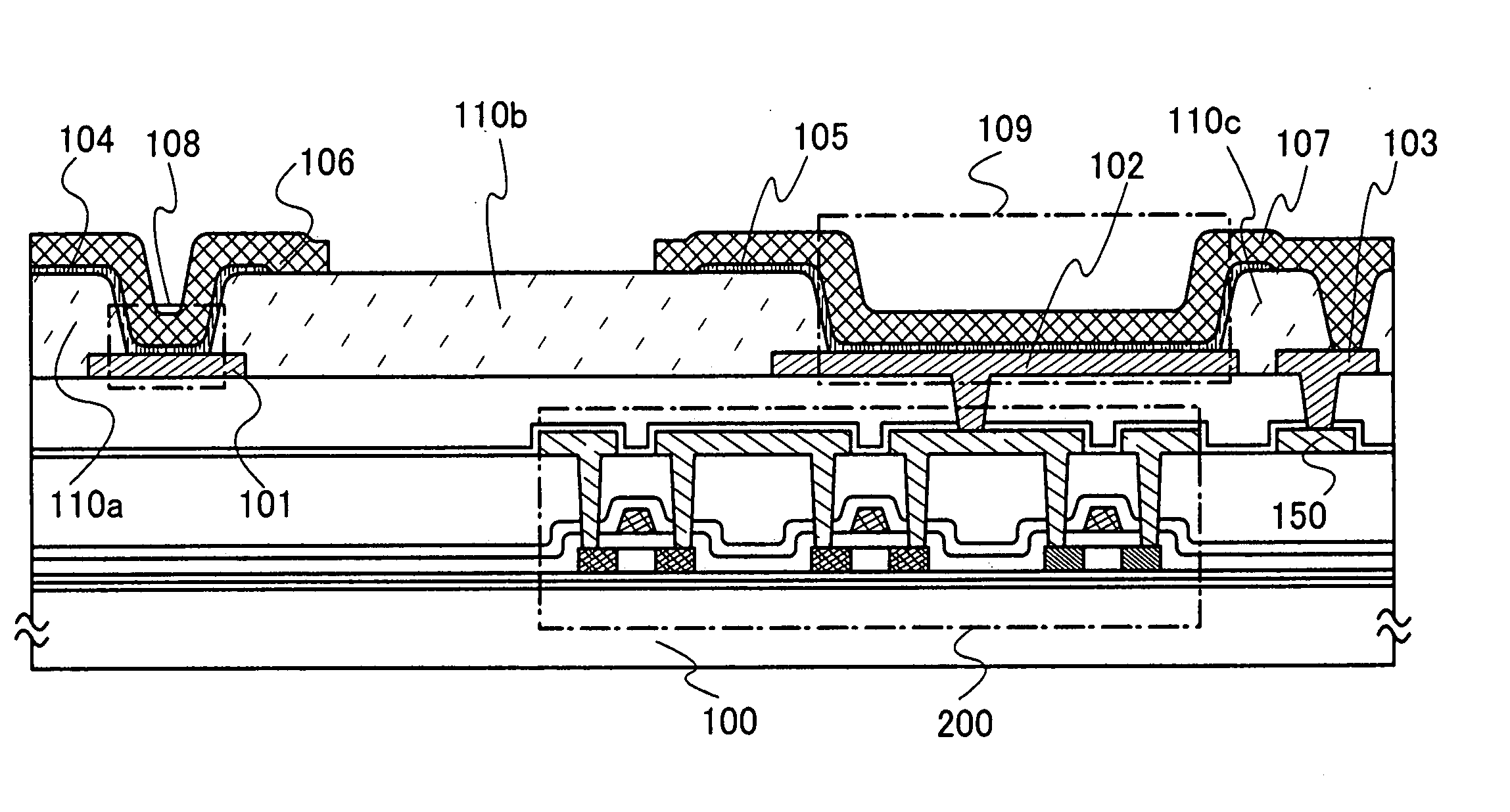
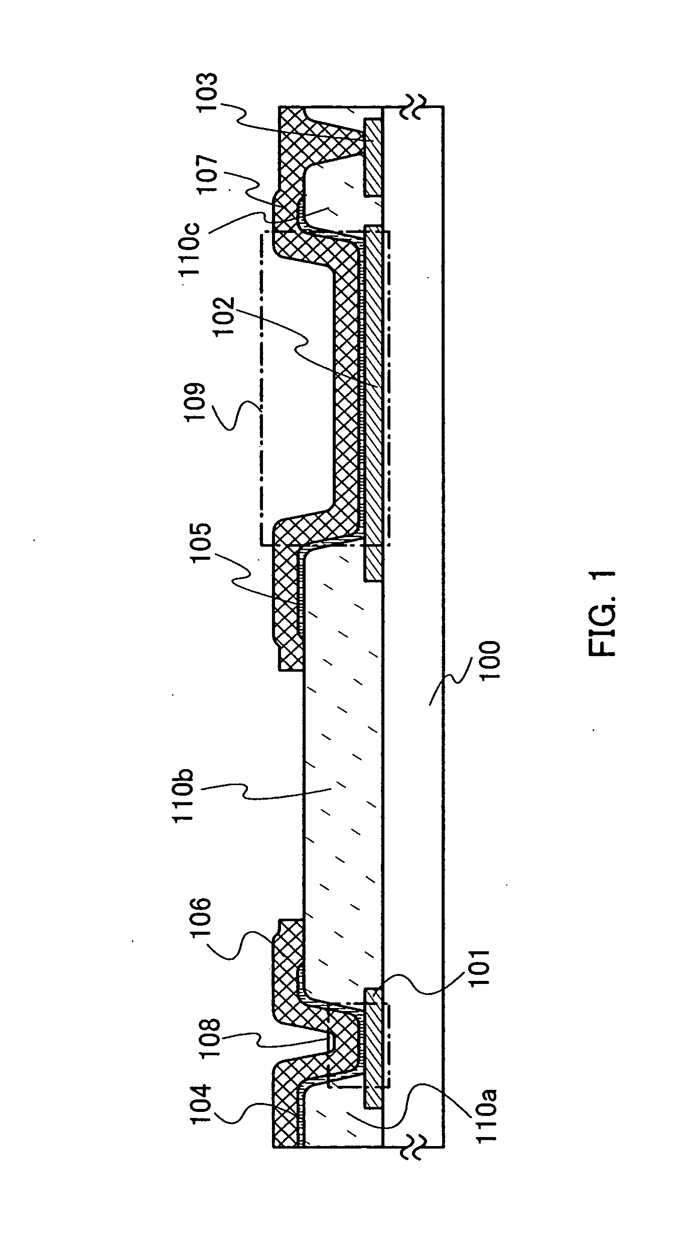
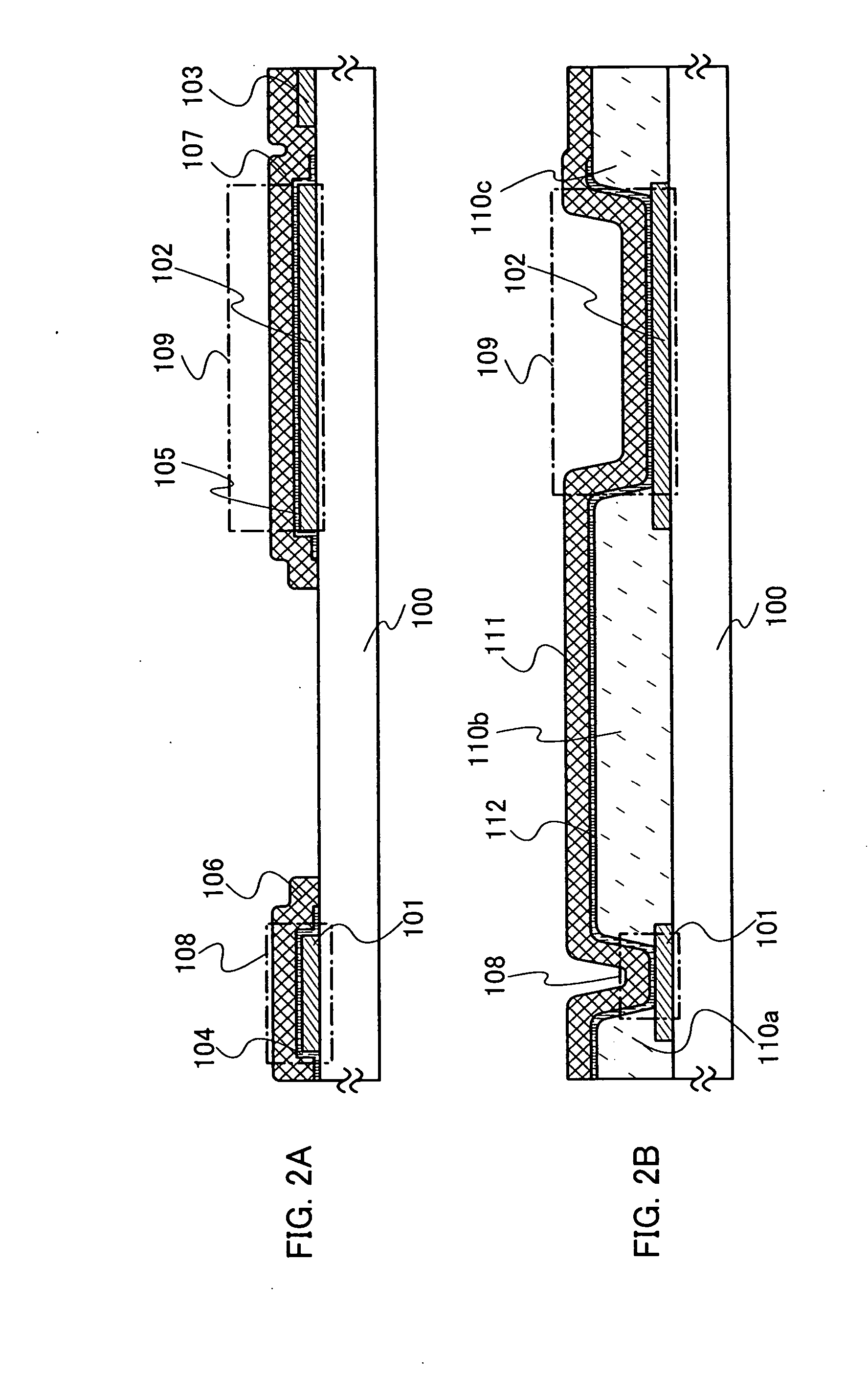
[0055] As for the semiconductor device related to the invention, a memory element 108 and a capacitor 109 are formed over a substrate 100 as shown in FIG. 1.

[0056] The memory element 108 shown in FIG. 1 is formed by stacking a first conductive layer 101, a layer containing an organic compound 104 and a second conductive layer 106. Further, the capacitor 109 is formed by stacking a first conductive layer 102, a layer containing an organic compound 105 using the same material as the memory element portion, and a second conductive layer 107. Partition layers 110a, 110b, and 110c have a function to prevent the first conductive laye...

embodiment mode 2

[0079] One structural example of a semiconductor device composed of a memory element in which a layer containing an organic compound is provided between two conductive layers and a capacitor in which the layer containing the organic compound which is the same as in the memory element is provided between two conductive layers is described with reference to drawings in this embodiment mode which is different from Embodiment Mode 1.

[0080] The structure in which the memory element 108 and the capacitor 109 are provided over the substrate 100 is shown in FIG. 1; however, the invention is not limited to this, and a transistor group 200 is provided over the substrate 100, and the memory element 108 and the capacitor 109 may be formed thereover as shown in FIG. 3. FIG. 3 shows a structure in which the capacitor 109 is formed just above the transistor group 200, and one end of an electrode is connected to a wiring 150. Accordingly, the capacitor 109 functions as capacity between the transis...

embodiment mode 3

[0091] One structural example of a semiconductor device composed of a memory element in which a layer containing an organic compound is provided between two conductive layers and a capacitor in which the layer containing the organic compound as in the memory element is provided between two conductive layers is described with reference to a drawing in this embodiment mode which is different from Embodiment Modes 1 and 2.

[0092] The capacitor of the invention can achieve the increase of capacity by combining an existing capacitor. FIG. 7 is an example in which a conventional capacitor using a semiconductor layer and a gate metal is combined with the capacitor of the invention.

[0093] In the example shown in FIG. 7, an existing capacitor 400 is formed over the substrate 100, and the memory element 108 and the capacitor 109 are formed thereover. The capacitor 400 is a capacitor which is used conventionally and in which a source electrode layer and a drain electrode layer of a TFT are co...


PUM


Abstract

An object of the invention is to reduce an area occupied by a capacitor in a circuit in a semiconductor device, and to downsize a semiconductor device on which the capacitor and an organic memory are mounted. The organic memory and the capacitor, included in a peripheral circuit, in which the same material as the layer containing the organic compound used for the organic memory is used as a dielectric, are used. The peripheral circuit here means a circuit having at least a capacitor such as a resonance circuit, a power supply circuit, a boosting circuit, a DA converter, or a protective circuit. Further, a capacitor in which a semiconductor is used as a dielectric may be provided over the same substrate as well as the capacitor in which the same material as the layer containing the organic compound is used as a dielectric. In this case, it is desirable that the capacitor in which the same material as the layer containing the organic compound is used as a dielectric and the capacitor in which the semiconductor is used as a dielectric are connected to each other in parallel.

Description

BACKGROUND OF THE INVENTION [0001] 1. Field of the Invention [0002] The present invention relates to a semiconductor device and a manufacturing method of the semiconductor device. Particularly, the invention relates to a semiconductor device which can store data by using an organic compound in a memory circuit and a capacitor. [0003] 2. Description of the Related Art [0004] In recent years, identification technology where an ID (identification number) is assigned to each object so as to reveal data thereon such as the history has been attracting attention, which is utilized for production management and the like. Above all, semiconductor devices capable of communicating data wirelessly have been developed. Such semiconductor devices include an RFID (Radio Frequency Identification) tag (also called an ID tag, an IC tag, an IC chip, an RF (Radio Frequency) tag, a wireless tag, an electronic tag, or a wireless chip), and the like have been introduced into companies, the market and the ...

Claims


Application Information

Patent Timeline
Patent Type & Authority Applications(United States)
IPC IPC(8): H01L29/00
CPCG11C5/025G11C8/08H01L27/105H01L27/28H01L27/1214H01L28/40H01L27/1052H01L27/12H01L27/1255H10B99/00H10K19/80H10K19/00
Inventor SAITO, TOSHIHIKO
Owner SEMICON ENERGY LAB CO LTD
Why Eureka
Try Eureka