Data conversion methods and systems

a data conversion and data technology, applied in the field ofsignal processing, can solve the problems of requiring an accurate analog path, limiting the resolution of the data conversion method to about 8 bits, and requiring serious “analog” bottlenecks in terms of accuracy and maximum speed of the converter, so as to reduce or eliminate critical analog circuit requirements and bottlenecks, improve dynamic range and quantization noise, and improve the effect of resolution

Inactive Publication Date: 2006-11-30
SPEEDARK
View PDF4 Cites 33 Cited by
  • Summary
  • Abstract
  • Description
  • Claims
  • Application Information

AI Technical Summary

Benefits of technology

[0021] According to the present invention there is provided a high-resolution, high-speed apparatus for data conversion, comprising: a first, low-resolution analog-to-digital converter (ADC1) operative to output a first digital output signal in a time domain; a first spectral signal processor operative to use a frequency domain to both convert the first digital output signal into an output analog subtraction signal and to provide a processed digital signal; a second low-resolution analog-to-digital converter (ADC2) operative to convert an analog error signal formed in a subtraction operation involving the output analog subtraction signal into a second digital output signal; and a digital combining unit operative to receive the processed digital signal and the second digital output signal and to combine both signals into a final digital output signal; whereby the apparatus has a higher resolution that either ADC1 or ADC1, and whereby the data conversion is performed in the frequency domain using frequency domain / spectral tools, thereby providing an improved dynamic range and quantization noise, a reduction or elimination of critical analog circuit requirements and bottlenecks, and an increase of the sampling rate relative to existing P / S architectures.
[0022] According to the present invention there is provided a method for implementing a high-performance converter comprising the steps of: processing a frequency domain signal and a time domain input signal using at least two data converters having each at least one lower performance parameter than the high-performance converter in order to obtain at least two processed signals, wherein the processing includes transforming the time domain input signal into the frequency domain signal in a digital form; dividing the frequency domain into at least two frequency domain parts, one part related to a low-resolution SNR, and another part related to a high-resolution SNR thereby extracting frequency domain information from the frequency domain signal in a digital form, and using it to obtain the at least two processed signals; and recombining the at least two processed signals to obtain a first final output signal from the high-performance converter, whereby the method provides higher performance and other advantages than comparable data conversion methods that work in the time domain
[0023] According to the present invention there is provided a method for implementing a high-performance analog-to-digital converter comprising the steps of: providing a first low-resolution analog-to-digital converter (ADC1) operative to convert an analog input signal into a first digital output signal in a time domain; providing a first spectral signal processor operative to process the first digital output signal and other received digital signals in a frequency domain and to provide a processed digital signal; providing a second low-resolution analog-to-digital converter (ADC2) operative to convert an analog error signal formed in a subtraction operation involving the output analog subtraction signal into a second digital output signal; and providing a digital combining unit operative to receive the processed digital signal and the second digital output signal and to combine both signals into a final digital output signal; whereby the analog-to-digital data conversion is performed preferably at least in part in the frequency domain using spectral tools, thereby providing an improved dynamic range and quantization noise, a reduction or elimination of critical analog circuit requirements and bottlenecks, and an increase of the sampling rate relative to existing P / S architectures.
[0024] The major components of the data converters disclosed herein are digital (with highly relaxed requirements for the remaining analog parts). Such data converters are expected to enjoy faster progress and better scaling of the digital technology in terms of performance, cost, power consumption, etc., in comparison with the existing analog technology.

Problems solved by technology

The main reasons for the slow advance are the bottlenecks of high-resolution / high-speed analog circuits.
The fastest ADC architecture is the Flash architecture, but its resolution is limited to about 8 bits by the number of comparators used.
A main disadvantage of this architecture is that it requires an accurate analog path that includes S / H units, subtractors and amplifiers.
This requirement is a serious “analog” bottleneck in terms of both accuracy and maximum speed of the converter.
Other ADC architectures such as Folding / Interpolating are also used at higher sampling rates, but they do not provide the resolution of the S / P architectures.
Use of parallel converters (time or frequency interleaving methods) increases the sampling rate, but comes at a cost of a linear increase in the number of converters in parallel.
Moreover, in addition to increased cost and matching difficulties, these architectures do not improve the basic converter resolution and / or dynamic range (DR).
The main disadvantage in Huang's method is that it operates only in a known communication channel and results in a relatively small improvement, which is also strongly dependent on the strong interferers characteristics.
The main disadvantage of all prior art DR reduction methods and systems is that they do not provide linear analog to digital conversion over the entire input DR.
Most of these methods and systems are also limited to specific applications.

Method used


Image

  • Data conversion methods and systems
  • Data conversion methods and systems
  • Data conversion methods and systems

Examples


Embodiment Construction

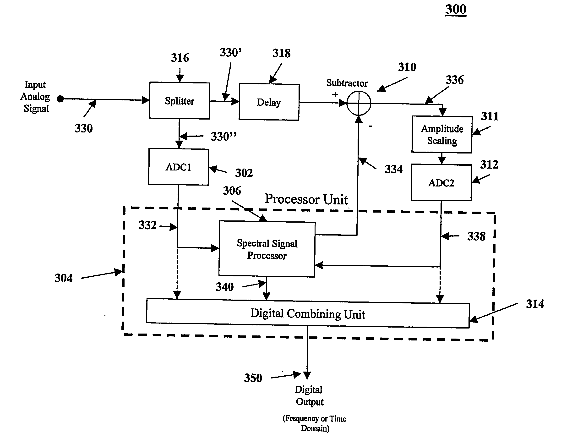
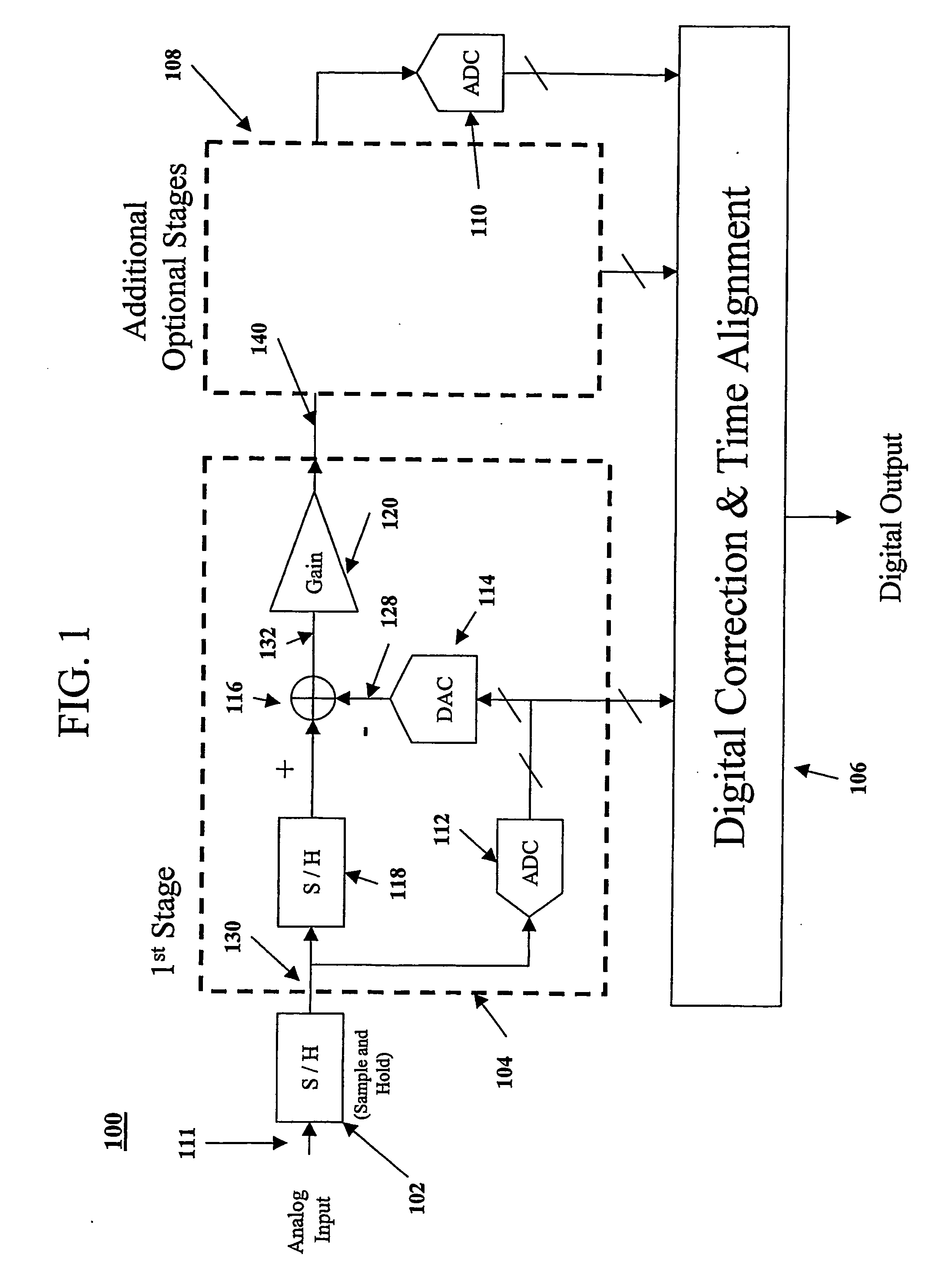
[0045] The present invention discloses new data conversion architectures and methods, with applications to high-speed, high-resolution ADCs and DACs. In this description, “system”, “apparatus” and “data conversion architecture” are used interchangeably. Also in the context of the present invention, the term “performance” represents the two basic data converter parameters: resolution and speed. “High-performance” means high-resolution and high. “Low performance” means low-resolution or low-speed or both. Typical exemplary ranges for “high” and “low” are given below.

[0046] In contrast with time domain concepts that serve most prior art data converter architectures, the data conversion architectures and methods disclosed herein use frequency domain tools to extract frequency domain information from the signal. This information is advantageously used in the processing of the signal, which is mainly digital.

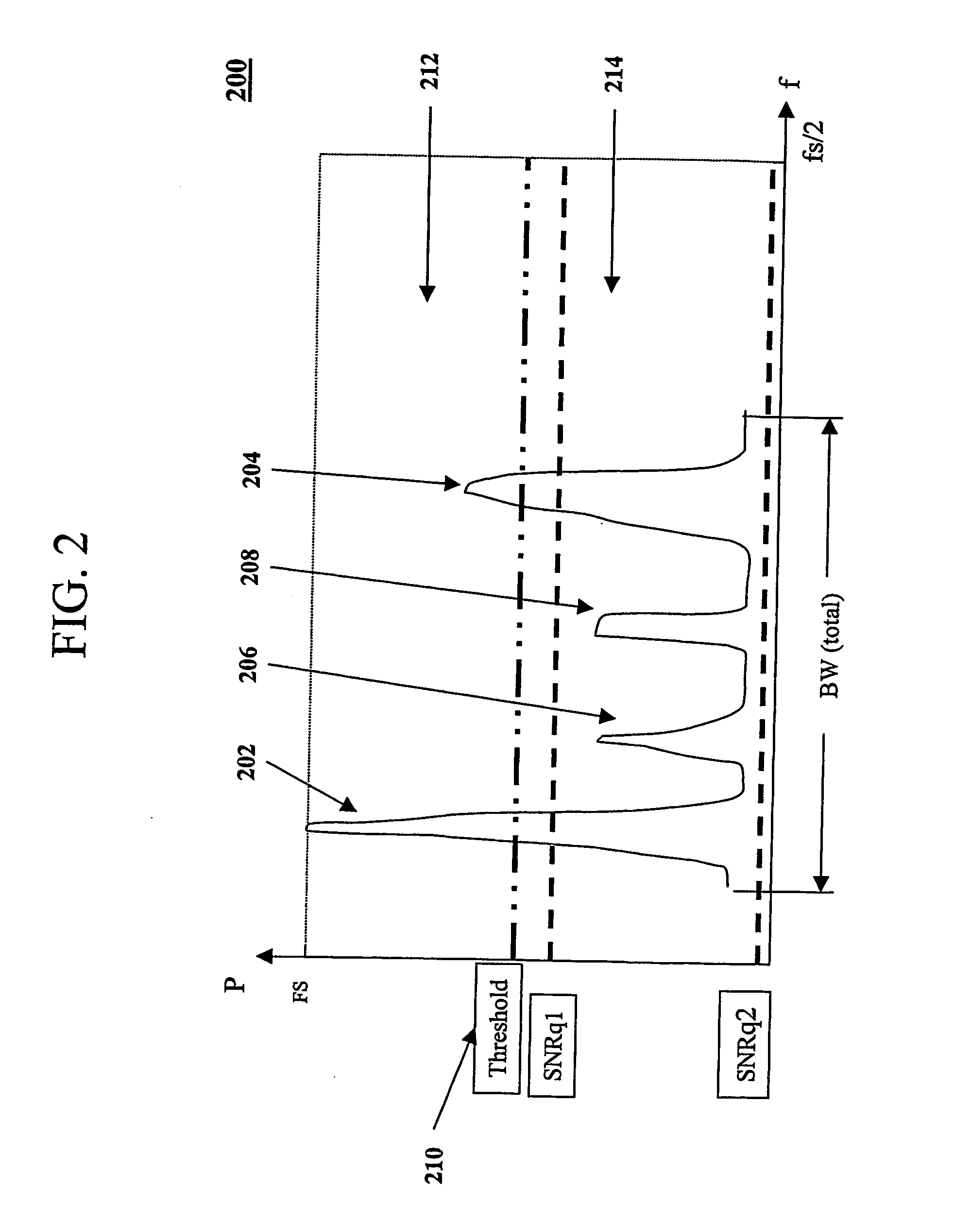
[0047]FIG. 2 shows the basic data conversion “spectral” concept of the present ...


PUM


Abstract

Methods and systems for implementing high-performance data converters remove analog technology bottlenecks and provide higher converter resolution and higher speed. A preferred embodiment of the method comprises the steps of transforming a time domain input signal into a frequency domain signal in a digital form, processing the frequency domain signal and the input signal using at least two lower-performance data converters in order to obtain at least two processed signals, and recombining the at least two processed signals to obtain a final output signal from the high-performance converter. Inventively and advantageously, the processing includes dividing the frequency domain into at least two frequency domain parts, one related to a low-resolution signal to noise ratio (SNR) and the other elated to a high-resolution SNR, and using frequency information resulting from the division to obtain the at least two processed signals.

Description

FIELD OF THE INVENTION [0001] The present invention relates to signal processing, particularly to data conversion methods and systems, and more particularly to analog-to-digital conversion and digital-to-analog conversion of signals. BACKGROUND OF THE INVENTION [0002] Data conversion is a critical technology in many applications. Analog-to-digital converter (ADC) technology is progressing much slower (˜1.5 Bits in 9 years, see e.g. R. H. Walden, “Performance trend for analog-to-digital converters,” IEEE Comm. Magazine, February 1999 pp. 96-101) than digital signal processing (DSP) technology (which follows Moore's law). The main reasons for the slow advance are the bottlenecks of high-resolution / high-speed analog circuits. Many commercial analog-to-digital converters (ADCs) today use a Pipeline / Subranging (P / S) architecture (see FIG. 1) to combine two or more low-resolution, high-speed ADCs in order to achieve high-resolution while maintaining wideband operation. [0003] Analog-to-di...

Claims


Application Information

Patent Timeline
Patent Type & Authority Applications(United States)
IPC IPC(8): H03M1/10G06FH03M1/06H03M1/14
CPCH03M1/145H03M1/06
Inventor BUNIN, HAIM
Owner SPEEDARK
Why Eureka
Try Eureka