Matched-impedance high-bandwidth configuration jumper

a high-bandwidth configuration, jumper technology, applied in the field of circuit boards, can solve the problems of inability to route high-speed lvds signals to multiple locations, zero-ohm resistors inevitably creating impedance discontinuities, and “impedance bumps", so as to prevent impedance discontinuities, improve signal transmission performance, and degrade the differential coupling ratio of differential signal conductor pairs

Active Publication Date: 2006-12-07
DELL PROD LP
View PDF2 Cites 15 Cited by
  • Summary
  • Abstract
  • Description
  • Claims
  • Application Information

AI Technical Summary

Benefits of technology

[0011] In one embodiment of the invention, the plurality of input pins and the plurality of output pins are adjacent to a plurality of ground pins to provide improved signal transmission performance. The geometry and spacing of the connection pins and the internal conductors are configured to provide a matched-impedance passthrough for differential signals to prevent impedance discontinuities that can create adverse signal reflections and degrade the intrapair differential coupling ratio of the differential signal conductor pairs.

Problems solved by technology

The connections used to transport high speed signals are generally point-to-point connections because the high speed signals cannot tolerate stubs that cause reflections and signal degradation.
In prior art circuit boards, it is not feasible to route high-speed LVDS signals to multiple locations.
Because of physical board routing constraints, routing the signals through zero-ohm resistors inevitably creates an impedance discontinuity, or “impedance bump” in the routing.
The impedance bump creates reflections along the signal and also degrades the intrapair differential coupling ratio, thereby increasing the effects of local EMI sources on the conductor pair.

Method used


Image

  • Matched-impedance high-bandwidth configuration jumper
  • Matched-impedance high-bandwidth configuration jumper
  • Matched-impedance high-bandwidth configuration jumper

Examples


Embodiment Construction

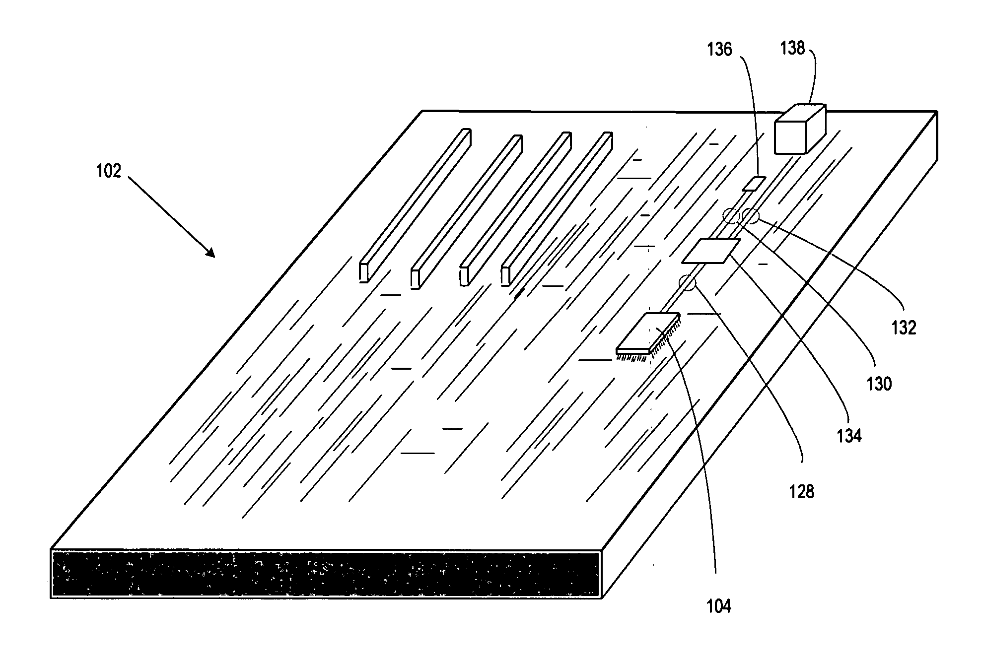
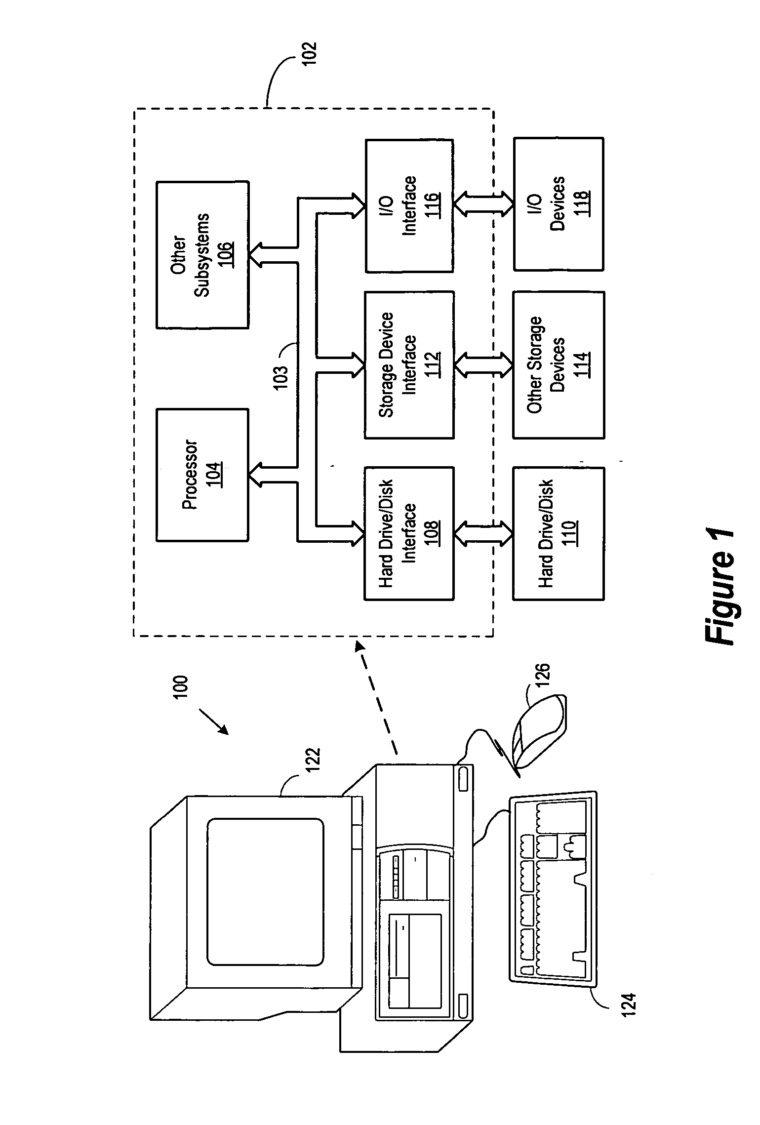
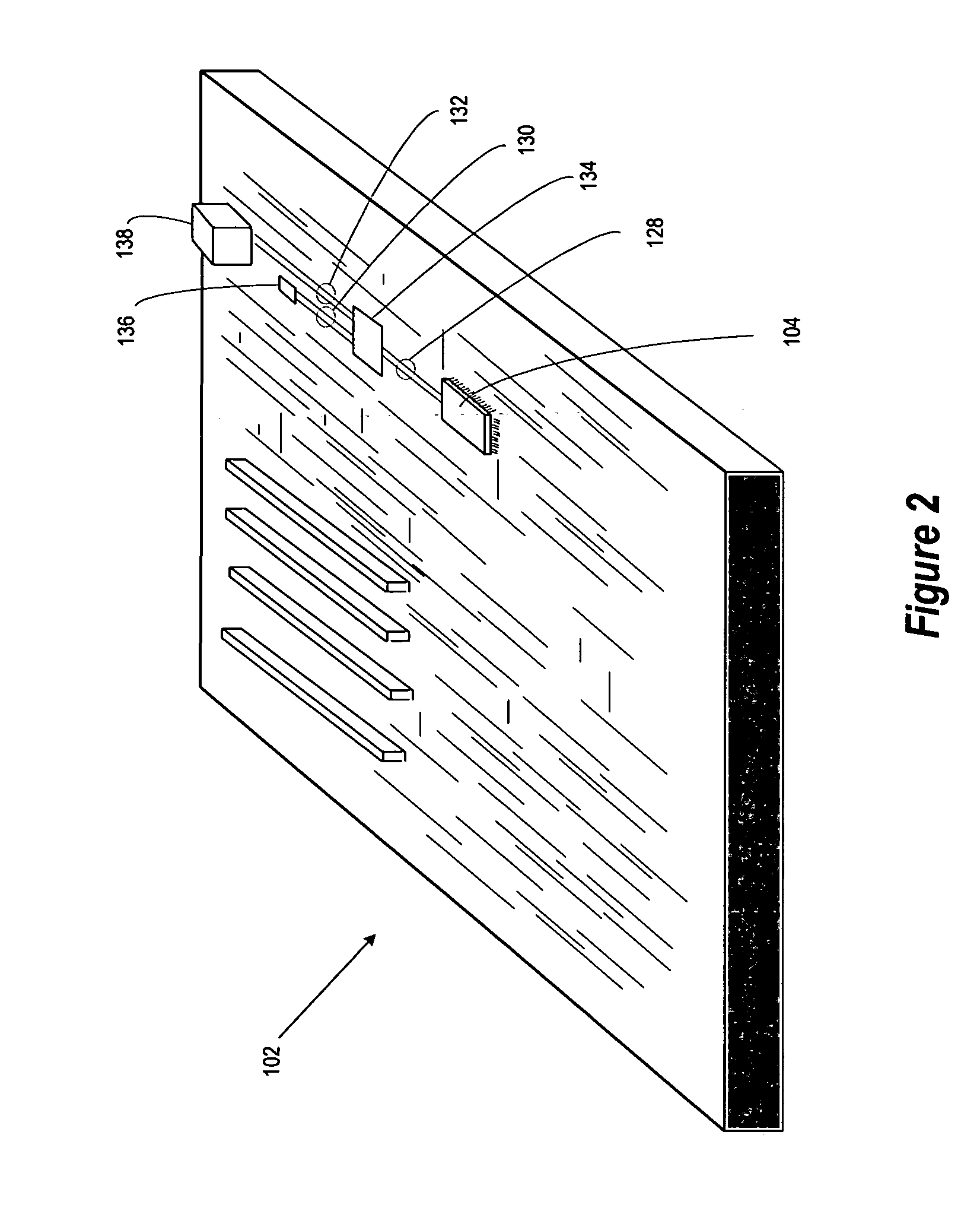
[0026] The method and apparatus of the present invention provides significant improvements in the manufacture and use of circuit boards such as those used in an information handling system 100 shown in FIG. 1. For purposes of this disclosure, an information handling system may include any instrumentality or aggregate of instrumentalities operable to compute, classify, process, transmit, receive, retrieve, originate, switch, store, display, manifest, detect, record, reproduce, handle, or utilize any form of information, intelligence, or data for business, scientific, control, or other purposes. For example, an information handling system may be a personal computer, a network storage device, or any other suitable device and may vary in size, shape, performance, functionality, and price. The information handling system may include random access memory (RAM), one or more processing resources such as a central processing unit (CPU) or hardware or software control logic, ROM, and / or other...


PUM


Abstract

The present invention provides a matched-impedance jumper that is operable to connect pairs of differential signal conductors to provide improved signal transmission characteristics. In an embodiment of the invention, the impedance-matched jumper is used to connect a first pair of differential signal conductors to a selected pair of differential signal conductors selected from a plurality of second pairs of differential signal conductors. The impedance-matched jumper comprises a plurality of input pins that are operable to connect with a plurality of connection pads on the first pair of differential signal conductors and a plurality of output pins operable to connect with a plurality of connection pads on the predetermined second pair of differential signal conductors. A plurality of internal conductors are operably connected to the input pins and the output pins to define a signal path therebetween. The signal path defined by the input pins, the output pins, and the internal conductors provides an impedance-matched passthrough for differential signals.

Description

BACKGROUND OF THE INVENTION [0001] 1. Field of the Invention [0002] The present invention relates generally to circuit boards used in information handling systems. More specifically, the present invention provides an improved method and apparatus for improving the signal transfer characteristics of conductors, particularly differential signal conductors, used on circuit boards in information handling systems. [0003] 2. Description of the Related Art [0004] As the value and use of information continues to increase, individuals and businesses seek additional ways to process and store information. One option available to users is information handling systems. An information handling system generally processes, compiles, stores, and / or communicates information or data for business, personal, or other purposes, thereby allowing users to take advantage of the value of the information. Because technology and information handling needs and requirements vary between different users or applic...

Claims


Application Information

Patent Timeline
Patent Type & Authority Applications(United States)
IPC IPC(8): H05K7/06H03H7/38
CPCG06F13/4086H05K1/0243H05K1/0245H05K2201/10363H05K3/222H05K2201/09236H05K1/025
Inventor CARRIER, PATRICK W.LOFFINK, JOHN S.
Owner DELL PROD LP
Why Eureka
Try Eureka