Manufacturing method of CMOS type semiconductor device, and CMOS type semiconductor device

a manufacturing method and semiconductor technology, applied in the direction of semiconductor devices, basic electric elements, electrical equipment, etc., can solve the problems of deteriorating nbti performance, enhanced boron penetration from a gate electrode to a silicon substrate, adverse effect of boron penetration on the performance of a pmos transistor, etc., to achieve the effect of improving the life of the nbti and enhancing the boron penetration

Active Publication Date: 2006-12-07
RENESAS ELECTRONICS CORP
View PDF6 Cites 11 Cited by
  • Summary
  • Abstract
  • Description
  • Claims
  • Application Information

AI Technical Summary

Benefits of technology

[0025] Further, since the CMOS type semiconductor device according to claim 9 comprises: a semiconductor substrate which has pMOS transistor areas and nMOS transistor areas; an insulating layer formed over the semiconductor substrate of the pMOS transistor areas; a high dielectric constant film which is formed over the insulating layer and including metal oxide components; and gate electrodes formed over the high dielectric constant film; wherein at least nitrogen and halogen are included at least at a part of the insulating layer; and a concentration of the halogen near the boundary of the semiconductor substrate and the insulating layer is higher than a concentration of the halogen near the boundary of the gate electrode and the high dielectric constant film, as a manufacturing method of the CMOS type semiconductor device which has an MOS structure which has a high dielectric constant film, it can be manufactured by the manufacturing method concerning claim 1. Therefore, improvement in NBTI life can be aimed at, without enhancing the boron penetration from the gate electrode.

Problems solved by technology

However, when boron was incorporated into a gate electrode of a pMOS transistor and the technology concerning above-mentioned Patent Reference 1 was applied, the following problem exists.
There is a problem that the boron penetration from a gate electrode to a silicon substrate is enhanced when such a situation occurs.
That is, the above-mentioned boron penetration to a semiconductor substrate has an adverse effect on the performance of a pMOS transistor.
When fluorine is implanted also to the gate insulating film of an nMOS transistor like this, the problem that the performance of the nMOS transistor concerned deteriorates (that is, the driving current of an nMOS transistor falls) will occur.

Method used


Image

  • Manufacturing method of CMOS type semiconductor device, and CMOS type semiconductor device
  • Manufacturing method of CMOS type semiconductor device, and CMOS type semiconductor device
  • Manufacturing method of CMOS type semiconductor device, and CMOS type semiconductor device

Examples


embodiment 1

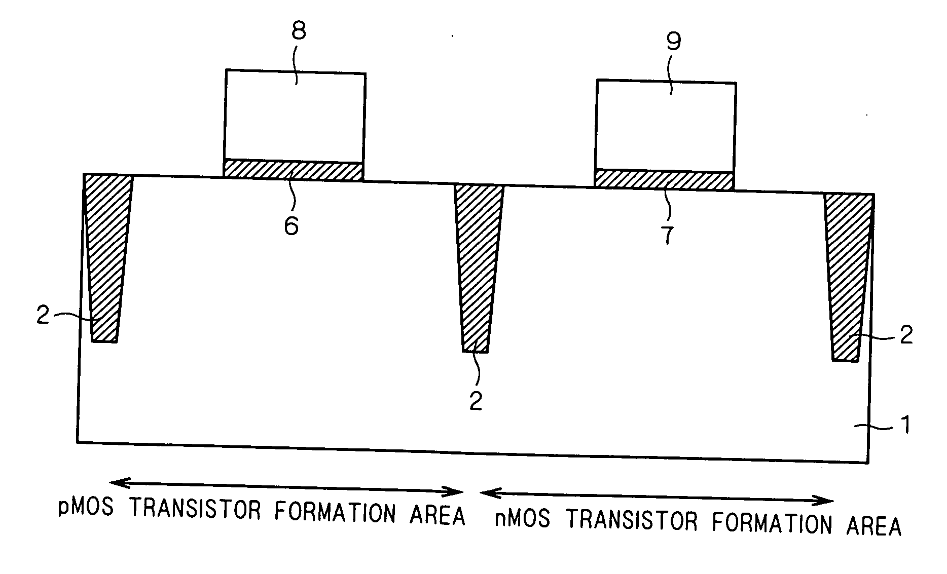
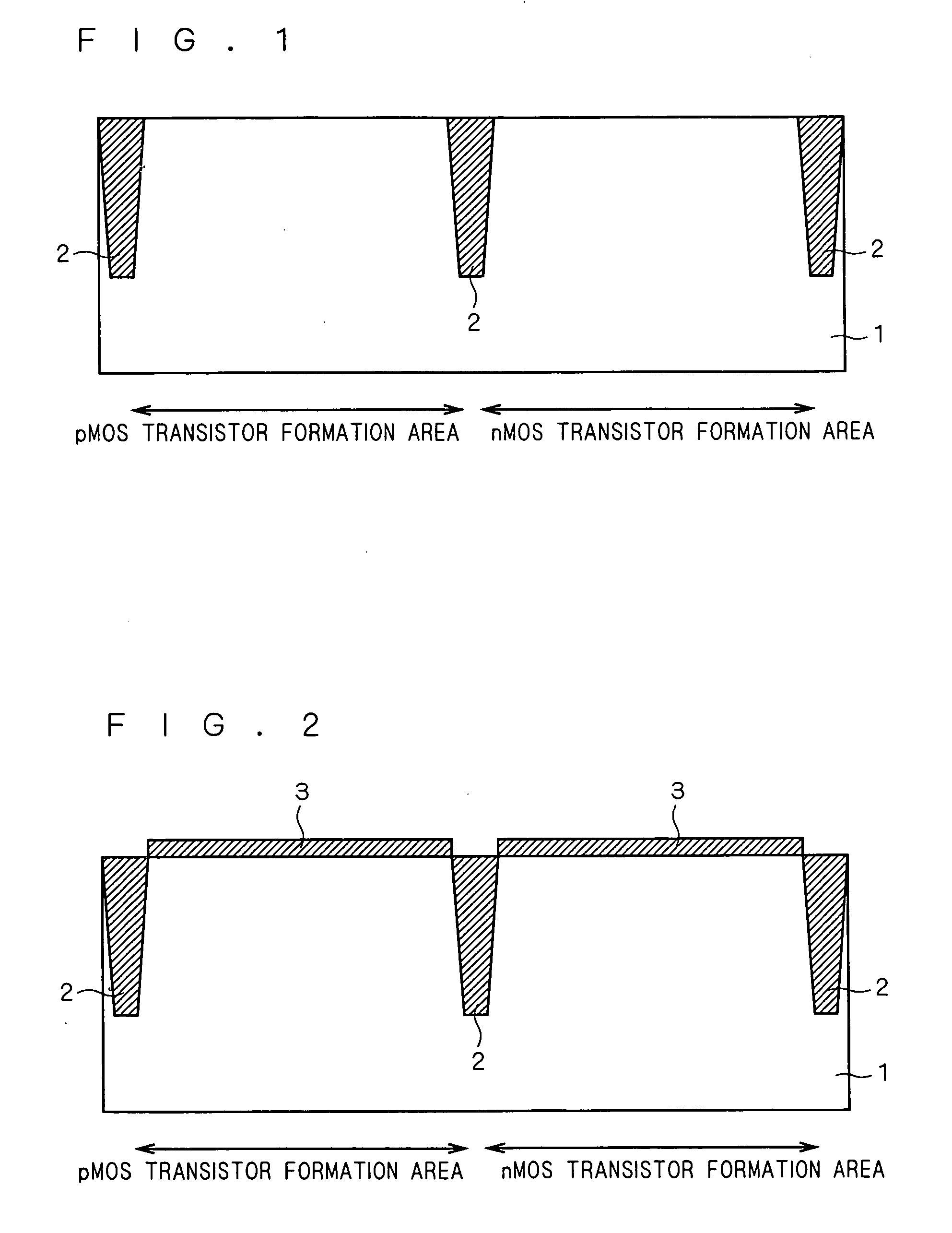
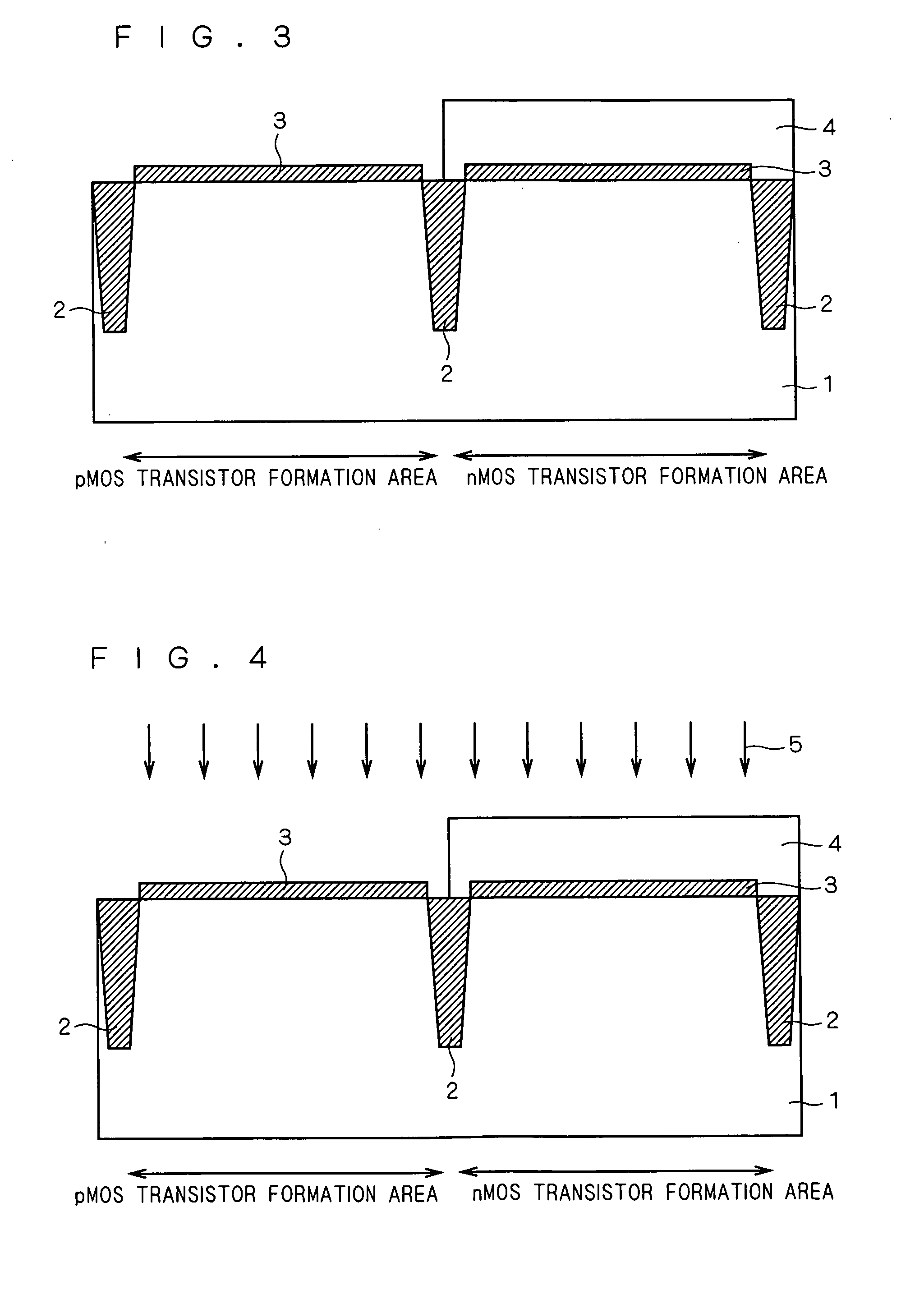
[0039] The manufacturing method of the CMOS type semiconductor device concerning this embodiment is concretely explained using process step sectional views.

[0040] First, as shown in FIG. 1, semiconductor substrate 1 which has a pMOS transistor formation area and an nMOS transistor formation area is prepared. Here, semiconductor substrate 1 is a p-type silicon substrate. Substrate of other types, such as n-type silicon or silicon on insulator (SOI) etc., can be used.

[0041] Next, as shown in FIG. 1, isolation 2 is formed in the surface of semiconductor substrate 1. A pMOS transistor formation area and an nMOS transistor formation area are electrically separated by the isolation 2 concerned. Here, the isolation 2 concerned can be formed by enforcing the shallow trench element isolation method, for example.

[0042] Next, n well (not shown) is formed to semiconductor substrate 1 of the pMOS transistor formation area. Further, p well (not shown) is formed to semiconductor substrate 1 of ...

embodiment 2

[0116] In Embodiment 1, reference was made about the case where only high-speed logic circuits are formed on a semiconductor substrate (that is, when forming the gate insulating film of one kind of thickness on a semiconductor substrate) for simplification of explanation.

[0117] However, generally as for the present leading edge semiconductor integrated circuit, two or more kinds of gate insulating films with which thickness differs are formed on a semiconductor substrate. For example, it is a case where it forms digital circuits which comprise high-speed logic circuits and input output circuits, a case where analog circuits are also formed besides digital circuits, etc.

[0118] In the above-mentioned exemplification, since high-speed operation is required, the gate insulating film of each MOS transistor of high-speed logic circuits is comparatively thin, and the thickness of the gate insulating film of the MOS transistors which forms the other circuits (input output circuit etc.) is...

embodiment 3

[0159] In this embodiment, the present invention (technology concretely concerning Embodiment 1) is applied in manufacture of the semiconductor device which has an MOS structure shown below.

[0160] Here, as for the above-mentioned MOS structure, a gate insulating film includes a high dielectric constant film. In the high dielectric constant film concerned, the oxide of one of metallic elements is contained, for example among metallic elements, such as Hf, Al, Zr, and La.

[0161] Thus, a high dielectric constant film is formed for the lowering of power consumption (suppression of leakage current) of the MOS transistor.

[0162] Hereafter, the manufacturing method concerning this embodiment is concretely explained using process step sectional views. Also in this embodiment, it explains as an example like Embodiment 2 bearing in mind manufacture of the digital type semiconductor integrated circuits with which high-speed logic circuits and input output circuits are formed on a semiconducto...


PUM


Abstract

The manufacturing method of the CMOS type semiconductor device which can suppress the boron penetration from the gate electrode of the pMOS transistors to the semiconductor substrate in the case that boron is contained in the gate electrodes, while enabling the improvement in the NBTI lifetime of the pMOS transistors, without degrading the performance of the nMOS transistors, is offered. The manufacturing method of the CMOS type semiconductor device concerning the present invention has the following process steps. Halogen is introduced to the semiconductor substrate of pMOS transistor formation areas. Next, a gate insulating film is formed on the semiconductor substrate of the pMOS transistor formation areas. Next, nitrogen is introduced to the gate insulating film.

Description

CROSS-REFERENCE TO RELATED APPLICATION [0001] The present application claims priority from Japanese patent application No. 2005-166609 filed on Jun. 7, 2005, the content of which is hereby incorporated by reference into this application. [0002] 1. Field of the Invention [0003] The present invention relates to a manufacturing method of a CMOS type semiconductor device, and a CMOS type semiconductor device, and particularly relates to a manufacturing method of a CMOS type semiconductor device, and a CMOS type semiconductor device with which nitrogen and halogen are included in a gate insulating film of a pMOS transistor. [0004] 2. Description of the Background Art [0005] Nitrogen is now commonly introduced into a gate insulating film in a CMOS type semiconductor device. It is from the following reasons to introduce nitrogen into a gate insulating film in this way. [0006] For example, it is assumed that a gate insulating film of the above-mentioned structure is formed on a semiconducto...

Claims


Application Information

Patent Timeline
Patent Type & Authority Applications(United States)
IPC IPC(8): H01L29/94
CPCH01L21/823857
Inventor TSUJIKAWA, SHIMPEIAKAMATSU, YASUHIKOUMEDA, HIROSHIYUGAMI, JIROMIZUTANI, MASAHARUINOUE, MASAOTSUCHIMOTO, JUNICHINOMURA, KOUJI
Owner RENESAS ELECTRONICS CORP
Why Eureka
Try Eureka