Method of designing an application specific probe card test system

a test system and probe card technology, applied in the direction of instrumentation, semiconductor/solid-state device testing/measurement, fault location by increasing destruction at fault, etc., can solve the problems of increasing the wear of the probe, operating software, and the increase of the cost of the replacement of the main test system controller components

Inactive Publication Date: 2006-12-07
FORMFACTOR INC
View PDF46 Cites 107 Cited by
  • Summary
  • Abstract
  • Description
  • Claims
  • Application Information

AI Technical Summary

Benefits of technology

[0024] In still further embodiments, only burn-in testing can be performed to limit the test system components needed, possibly eliminating the need for a complex ATE type test system controller. Test circuitry can be provided on the probe card, along with an external power supply and a personal computer to interface with the test circuitry to eliminate the need for the ATE type tester.

Problems solved by technology

Cost considerations for the test equipment are also important, so designers typically attempt to make only test signal software changes and changes to the probe cards to accommodate different wafer layouts, since replacement of the main test system controller components and operating software are significantly more expensive.
A limitation of a typical test system controller with increased density of DUTs on a wafer is that not all DUTs can be tested during a single touch down of a probe card.
Multiple touch downs, however, may be undesirable since touchdowns increase the likelihood of damaging the wafer, and touch downs further increase wear on the probes in the test system, which may be expensive to replace.

Method used


Image

  • Method of designing an application specific probe card test system
  • Method of designing an application specific probe card test system
  • Method of designing an application specific probe card test system

Examples


Embodiment Construction

I. Probe Card with On-Board Intelligent Circuitry

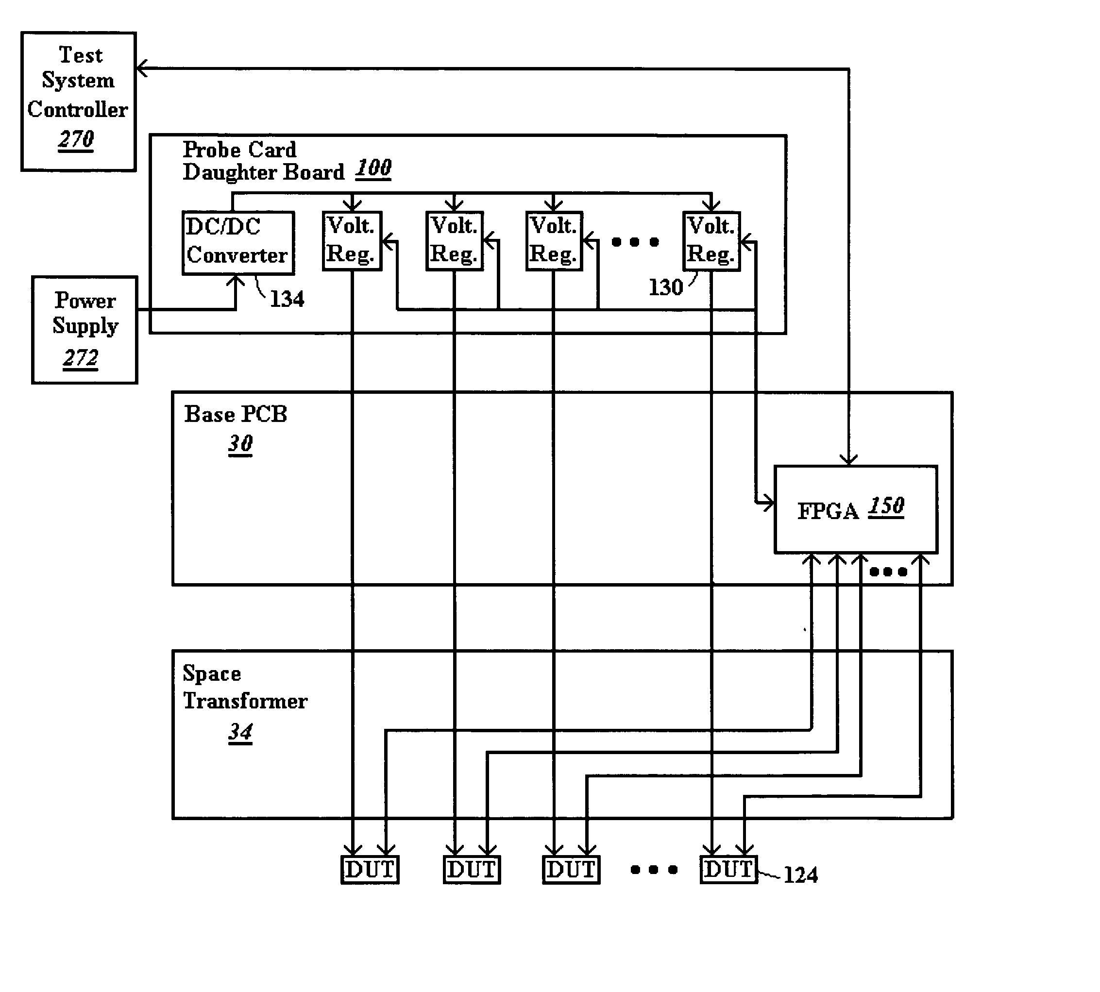
[0040]FIG. 6 shows a cross sectional view of a probe card, modified from the probe card configuration shown in FIG. 3 to include on board components that can be programmed to perform testing in accordance with some embodiments of the present invention. The probe card includes two daughter cards 100. For convenience, components carried over from FIG. 3 to FIG. 6 are similarly labeled. The daughter cards 100 are shown in FIG. 6 as connected by stacked connectors 1041-4. Although two daughter cards 100 are shown, a single card, more than two cards, or only a PCB without daughter cards 100 can be used to support on-board intelligent circuitry.

[0041] As illustrated, the daughter cards 100 can be provided in available spacing between test system controller interface connectors 24. The test system controller (not shown) attached using connectors 24 can limit the height above the connectors 24 within which the daughter cards can be stacked. ...


PUM


Abstract

A method is provided for design and programming of a probe card with an on-board programmable controller in a wafer test system. Consideration of introduction of the programmable controller is included in a CAD wafer layout and probe card design process. The CAD design is further loaded into the programmable controller, such as an FPGA to program it: (1) to control direction of signals to particular ICs, even during the test process (2) to generate test vector signals to provide to the ICs, and (3) to receive test signals and process test results from the received signals. In some embodiments, burn-in only testing is provided to limit test system circuitry needed so that with a programmable controller on the probe card, text equipment external to the probe card can be eliminated or significantly reduced from conventional test equipment.

Description

CROSS-REFERENCE TO RELATED APPLICATION [0001] The present application is a continuation-in-part of application Ser. No. 10 / 828,755, filed Apr. 21, 2004, entitled “Intelligent Probe Card Architecture,” by Miller, et al., which is incorporated by reference herein in its entirety.BACKGROUND [0002] 1. Technical Field [0003] Embodiments of the present invention relate to programming of test systems with probe cards. More particularly, embodiments of the present invention relate to probe cards with on board features used to test integrated circuits (ICs) on a wafer. [0004] 2. Related Art [0005] A wafer testing device typically includes a probe card with probes for electrically contacting pads of ICs on the wafer. The location of the IC contact pads on a wafer, as well as the signals that need to be sent for testing are different for each IC design. In the test system, the length of test lines and components on the probe card should also be considered to best interpret test results. Cost c...

Claims


Application Information

Patent Timeline
Patent Type & Authority Applications(United States)
IPC IPC(8): G01R31/02G01R1/073G01R1/36G01R31/28G01R31/319G01R35/00
CPCG01R31/2889G01R35/00G01R31/31926G01R31/31905G01R1/073H01L22/00
Inventor MILLER, CHARLES A.CHRAFT, MATTHEW E.HENSON, ROY J.
Owner FORMFACTOR INC
Why Eureka
Try Eureka