Thermally conductive ceramic tipped contact thermocouple

a ceramic and contact thermocouple technology, applied in the direction of heat measurement, semiconductor/solid-state device testing/measurement, instruments, etc., can solve problems such as contamination problems, failure of integrated circuits, and mechanical strength

Inactive Publication Date: 2006-12-07
APPLIED MATERIALS INC
View PDF15 Cites 324 Cited by
  • Summary
  • Abstract
  • Description
  • Claims
  • Application Information

AI Technical Summary

Problems solved by technology

One challenge in this area has been to develop a Si, C, and O containing film that has a low k value and also exhibits desirable thermal and mechanical properties.
Often Si, C, and O containing films that have a desirable dielectric constant exhibit poor mechanical strength and are easily damaged by

Method used


Image

  • Thermally conductive ceramic tipped contact thermocouple
  • Thermally conductive ceramic tipped contact thermocouple
  • Thermally conductive ceramic tipped contact thermocouple

Examples


Embodiment Construction

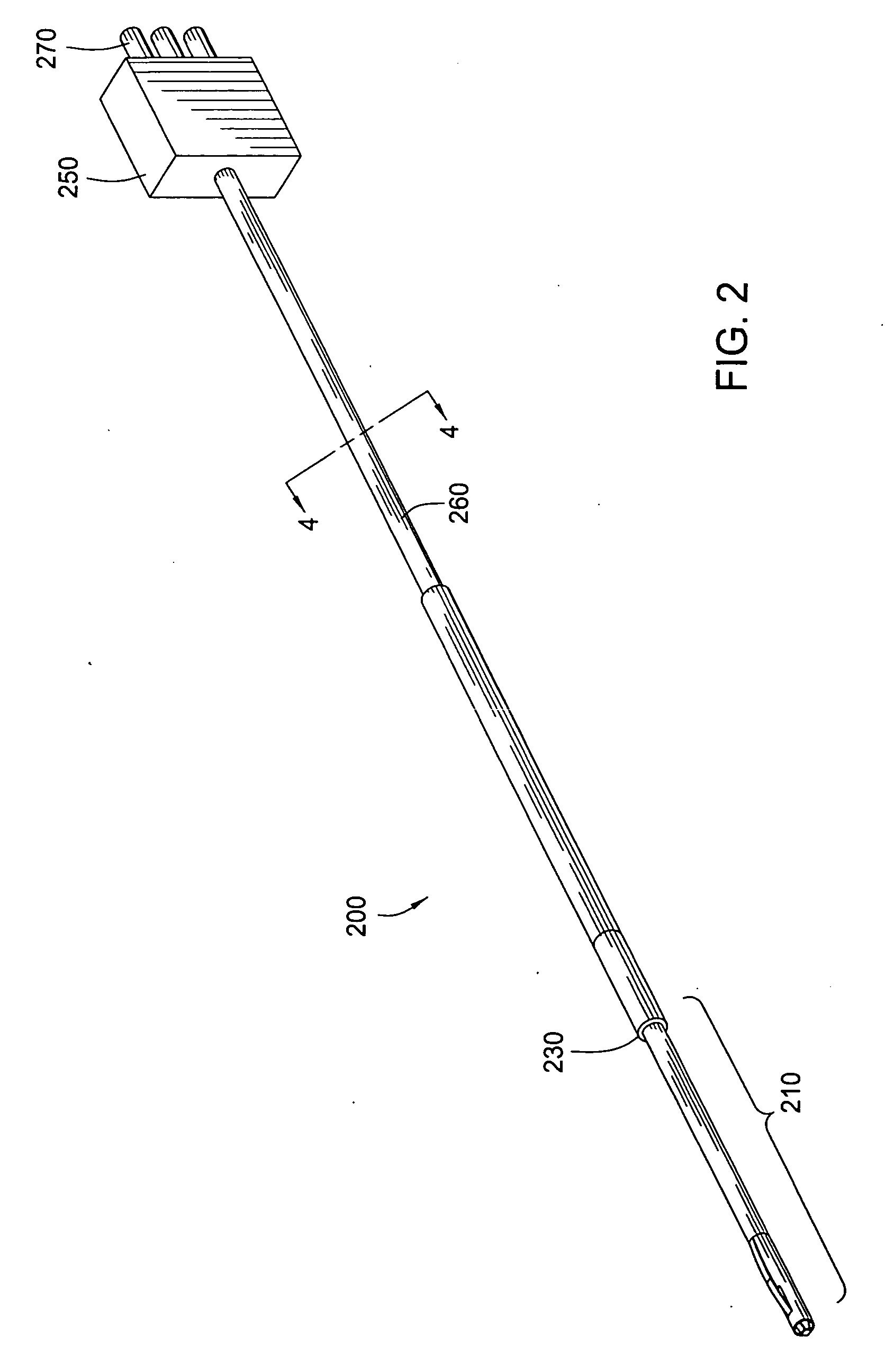
[0022] Embodiments of the present invention provide a thermocouple assembly comprising a ceramic tip. These embodiments may be used in other processing chambers including but not limited to CVD, PVD, PECVD or any other processing or manufacturing chambers requiring temperature monitoring.

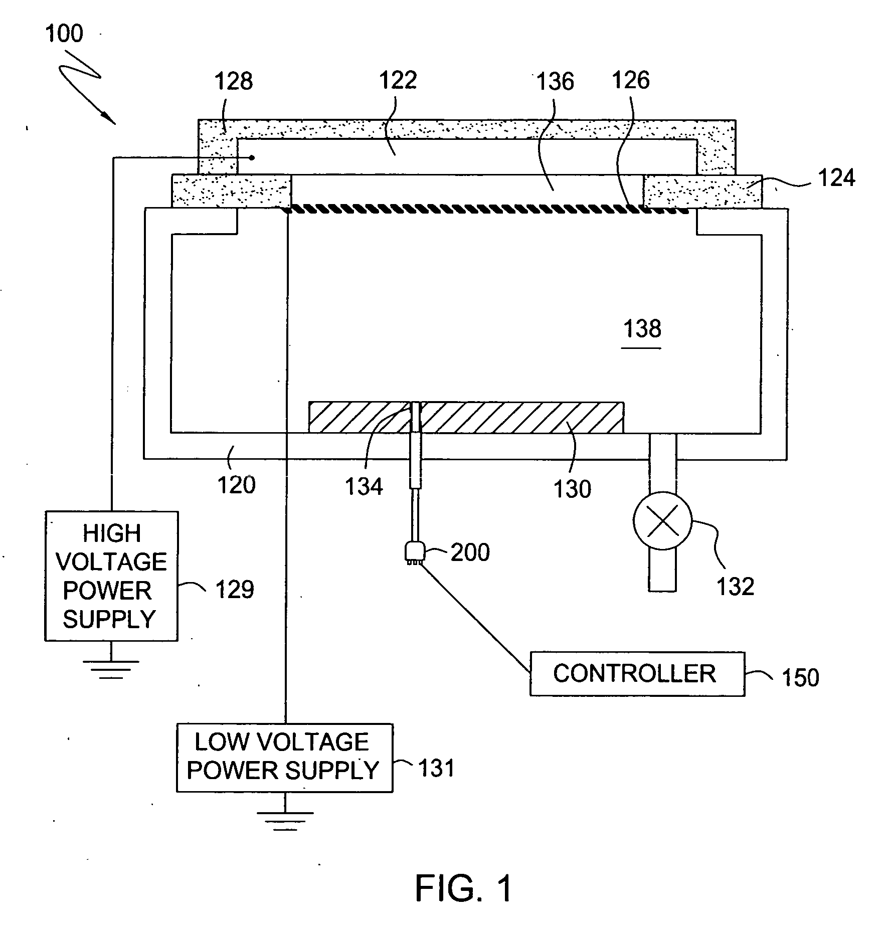
[0023]FIG. 1 is a cross-sectional diagram of an exemplary processing chamber 100, the e-beam chamber, in accordance with an embodiment of the invention. The e-beam chamber 100 includes a vacuum chamber 120, a large-area cathode 122, a target plane or substrate support 130 located in a field-free region 138, and a grid anode 126 positioned between the target plane 130 and the large-area cathode 122. The target plane 130 contains at least one hole 134 that extends through the vacuum chamber 120, for embedding a temperature measuring element such as a thermocouple assembly 200. The thermocouple assembly 200 is connected to a controller 150. The e-beam chamber 100 further includes a high voltage insula...


PUM


Abstract

An apparatus for processing a substrate. The apparatus comprising a tubular member with a first end and a second end. The first end comprising an opening; and a temperature sensor disposed in the opening. The temperature sensor comprising a resilient member. The resilient member comprising a surface made of a ceramic material wherein the surface made of a ceramic material extends through the opening to provide a substrate contact surface.

Description

BACKGROUND OF THE INVENTION [0001] 1. Field of the Invention [0002] Embodiments of the present invention generally relate to temperature measurement technology. More particularly, embodiments of the present invention relate to a device for temperature measurement in a semiconductor processing environment. [0003] 2. Description of the Related Art [0004] Semiconductor device geometries have dramatically decreased in size since such devices were first introduced several decades ago. Since then, integrated circuits have generally followed the two year / half-size rule (often called Moore's Law), which means that the number of devices that will fit on a chip doubles every two years. Today's fabrication plants are routinely producing devices having 0.13 μm and even 0.1 μm feature sizes, and tomorrow's plants will soon be producing devices having even smaller geometries. [0005] In order to further reduce the size of devices on integrated circuits; it has become necessary to use conductive ma...

Claims


Application Information

Patent Timeline
IPC IPC(8): H01L21/66H01L23/58G01K7/00
CPCG01K1/143H01L21/67248G01K1/16
Inventor DU BOIS, DALE R.ROCHA-ALVAREZ, JUAN CARLOS
Owner APPLIED MATERIALS INC
Why Eureka
Try Eureka