Method of fabricating light-emitting semiconductor device

a technology of semiconductor devices and semiconductors, applied in the field of light-emitting diodes, can solve the problems of not contributing to the net efficiency of light-emitting devices, corresponding drop in light production efficiency, and waste of current flowing in this part of the active layer, so as to promote lateral spreading current, low lateral resistivity, and high light production efficiency

Inactive Publication Date: 2006-12-07
SANKEN ELECTRIC CO LTD
View PDF14 Cites 10 Cited by
  • Summary
  • Abstract
  • Description
  • Claims
  • Application Information

AI Technical Summary

Benefits of technology

[0010] Briefly, the invention may be summarized as a light-emitting semiconductor device of improved efficiency. Included is a lamination of: (a) a first compound semiconductor layer of a first conductivity type; (b) an active layer of a compound semiconductor on the first compound semi-conductor layer; (c) a transparent second compound semiconductor layer of a second conductivity type, opposite to the first conductivity type, on the active layer; and (d) a transparent current spreading layer on the second compound semiconductor layer. An electrode is electrically coupled to the current spreading layer so as to permit emission of light radiated from the active layer through the current spreading layer. Another electrode is electrically coupled to the first compound semiconductor layer.
[0020] 2. If the multiple heterojunction current spreading layer according to the invention is to offer the same degree of uniformity in lateral current distribution as heretofore, this layer can be significantly less in thickness than its conventional counterpart. Such a thinner current spreading layer will less hinder the passage of light therethrough and incur less power loss.

Problems solved by technology

The current flowing in this part of the active layer was wasted, not contributing to the net efficiency of the light emitting device.
Itself impervious to light, however, the annulus reduced by as much as 30 to 40 percent the surface area from which light was emitted, causing a corresponding drop in the efficiency of light production.
Additionally, the current spreading layer was not nearly so pervious to light as could be desired, absorbing so much light as to invite a significant diminution in the efficiency of light production.
The relatively thick current spreading layer proposed by the U.S. patent cited above is also objectionable from the standpoint of maximal light emission.
This layer has proved to absorb so much light as to cause a significant decrease in the efficiency of light emission.

Method used


Image

  • Method of fabricating light-emitting semiconductor device
  • Method of fabricating light-emitting semiconductor device
  • Method of fabricating light-emitting semiconductor device

Examples


embodiment

of FIG. 4

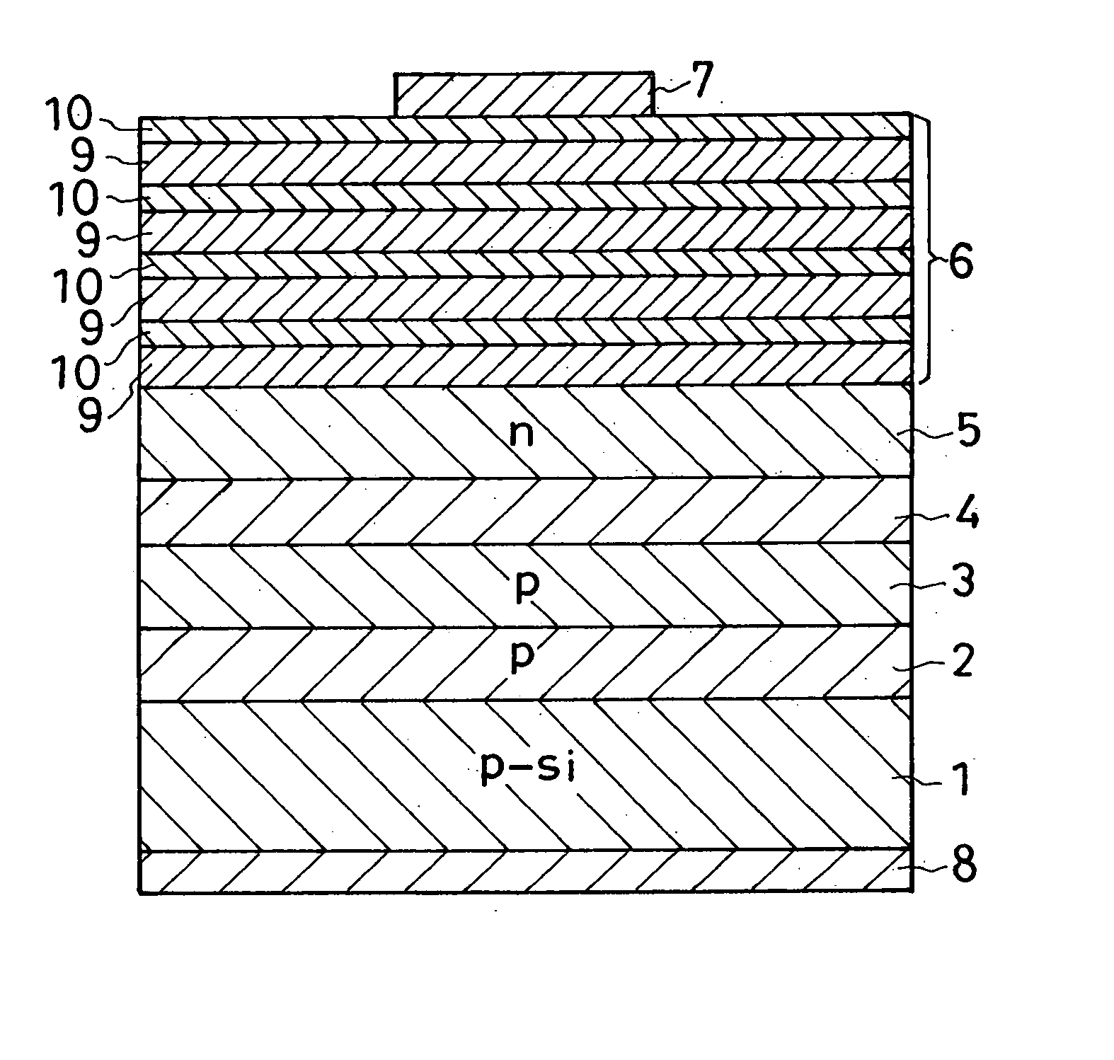
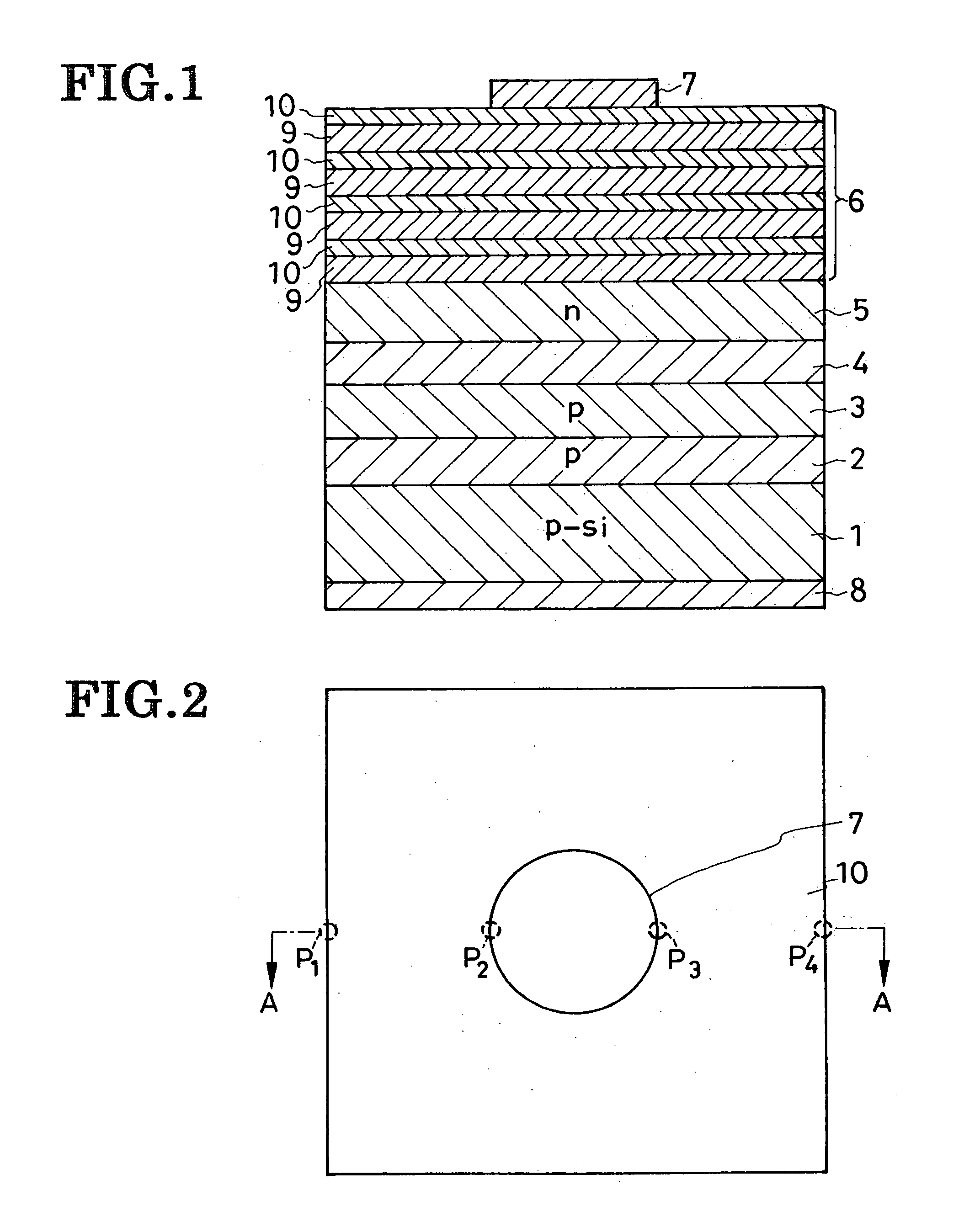
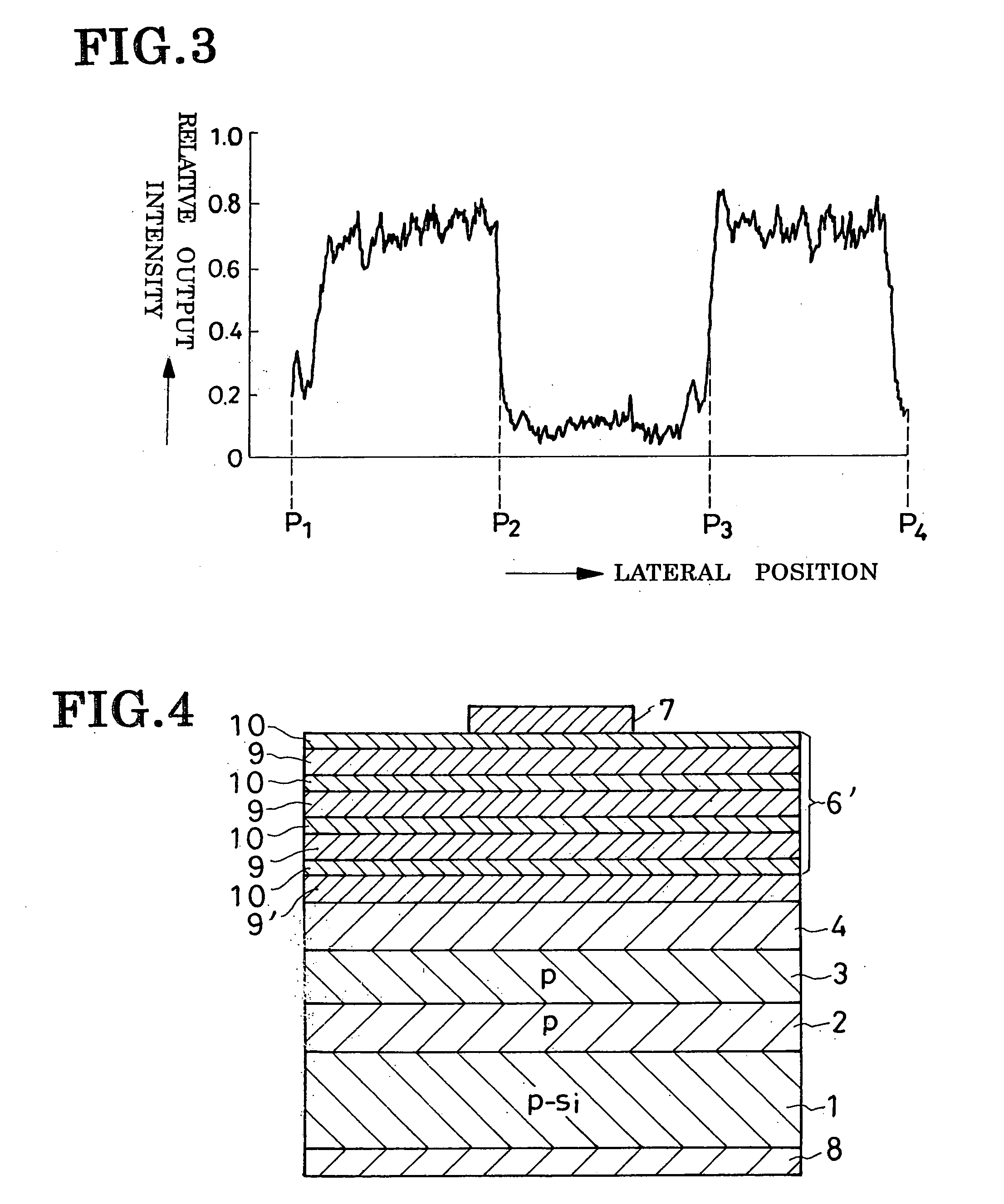
[0068] Another preferred form of LED shown in FIG. 4 is akin to that of FIGS. 1 and 2 except for the absence of the n-type nitride semiconductor layer 5. Formed on the active layer 4 in lieu of the missing n-type nitride semiconductor layer 5 is an n-type nitride semiconductor layer 9′ which is of the same composition as the first sublayers 9 of the current spreading layer. This current spreading layer is generally designated 6′ in FIG. 4 because of the absence of the lowermost first sublayer 9.

[0069] Thus the n-type nitride semiconductor layer 9′ is in contact both with one second sublayer 10 of the current spreading layer 6′ in order to offer the two-dimensional electron gas effect, and with the active layer 4 in order to function as n-type cladding like the n-type nitride semiconductor layer 5 of the FIGS. 1 and 2 embodiment. The current spreading layer 6′ is similar in construction to its FIG. 1 counterpart 6 except for the absence of the lowermost first sublayer 9. Th...


PUM


Abstract

A light-emitting diode having a silicon substrate on which there are successively formed a buffer layer, a p-type nitride semiconductor layer, an active layer, an n-type nitride semiconductor layer, and a current spreading layer. The current spreading layer is a lamination of a first and a second sublayer arranged alternately a required number of times. Composed of different compound semiconductors, the alternating sublayers of the current spreading layer create heterojunctions for offering the two-dimensional gas effect. The current spreading layer is so low in resistivity in a direction parallel to its major surface from which light is emitted, that the current is favorably spread therein for improved efficiency of light emission. A front electrode in the form of a metal pad is mounted centrally on the major surface of the current spreading layer in ohmic contact therewith.

Description

CROSS-REFERENCE TO RELATED APPLICATIONS [0001] This application is a Divisional of U.S. application Ser. No. 10 / 994,922 filed Nov. 22, 2004 (Atty. Docket No. TAK-0404), which claims priority to Japanese Patent Application No.2003-396151, filed Nov. 26, 2003.FIELD OF THE INVENTION [0002] This invention relates to a light-emitting diode or like semiconductor device made from chemical compounds, particularly those of Groups III-V elements, and to a method of making such a light-emitting device. BACKGROUND OF THE INVENTION [0003] A typical conventional compound semiconductor light-emitting device is a lamination of a baseplate of sapphire or silicon carbide or silicon, a buffer layer, an n-type semiconductor layer, an active layer, a p-type semiconductor layer, and a contact layer. Another example, taught by the U.S. Pat. No. 5,008,718 to Fletcher et al., is a lamination of a substrate, an n-type semiconductor layer, an active layer, a p-type semiconductor layer, and a current spreading...

Claims


Application Information

Patent Timeline
Patent Type & Authority Applications(United States)
IPC IPC(8): H01L21/00H01L33/00H01L33/04H01L33/14
CPCH01L33/007H01L33/14H01L33/04
Inventor AOYAGI, HIDEKAZUOTSUKA, KOJISATO, MASAHIRO
Owner SANKEN ELECTRIC CO LTD
Why Eureka
Try Eureka