EEPROM cell and EEPROM block

a technology of eeprom and eeprom block, which is applied in the field of nonvolatile memory, can solve the problems of inefficiency and economic problems of selection transistors, structure using row/column decoders, etc., and achieve the effect of saving the manufacturing cost of an overall chip

Active Publication Date: 2006-12-21
MAGNACHIP SEMICONDUCTOR LTD
View PDF7 Cites 6 Cited by
  • Summary
  • Abstract
  • Description
  • Claims
  • Application Information

AI Technical Summary

Benefits of technology

[0005] It is, therefore, an object of the present invention to provide an embedded EEPROM cell that can save manufacturing cost of an overall chip and an EEPROM block having the same.

Problems solved by technology

In these applications, such a conventional structure using the row / column decoder and the selection transistor is inefficient and not economical.

Method used


Image

  • EEPROM cell and EEPROM block
  • EEPROM cell and EEPROM block
  • EEPROM cell and EEPROM block

Examples


Embodiment Construction

[0019] Hereinafter, preferred embodiments of the present invention will be set forth in detail with reference to the accompanying drawings. First, it should be noted that the terms and words used in the specification and claims should not be limited to general or dictionary meanings but be interpreted as meanings and concepts which coincide with the technical spirit of the invention under the principle that the inventor(s) may properly define the concept of the terms to explain his / her own invention in the best way. Accordingly, the embodiments disclosed herein and constructions shown in the drawings don't teach all of the technical spirit of the invention but are merely the most preferred ones of the invention. Therefore, those in the art will appreciate that various modifications, substitutions and equivalences may be made, without departing from the scope of the invention as defined in the accompanying claims.

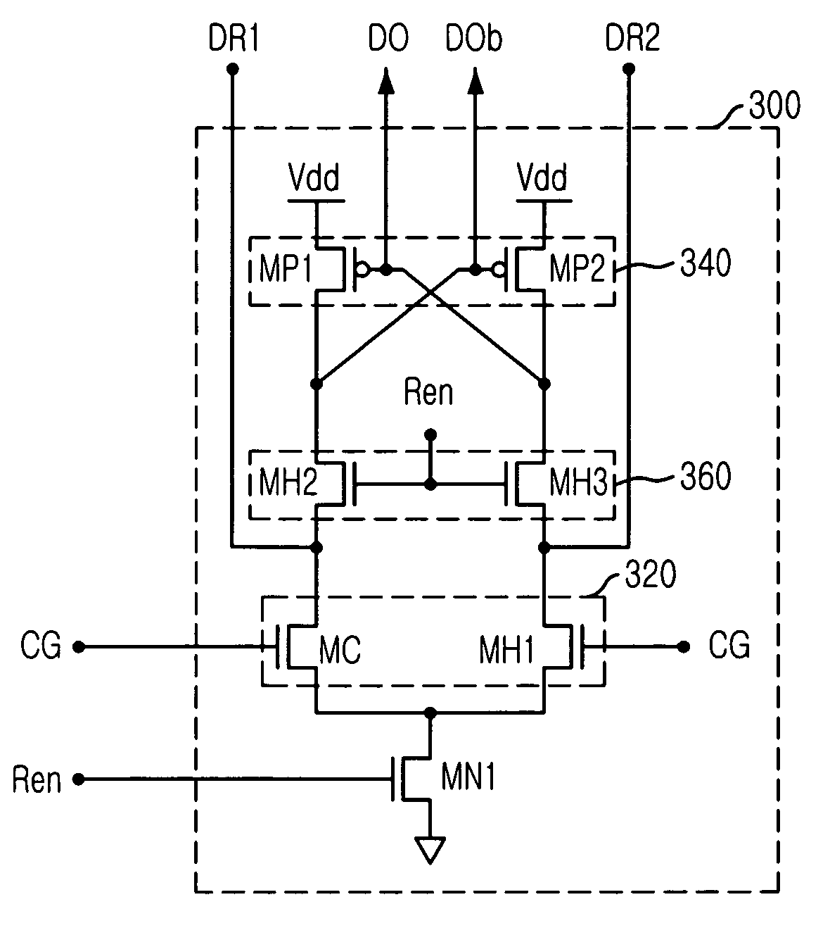
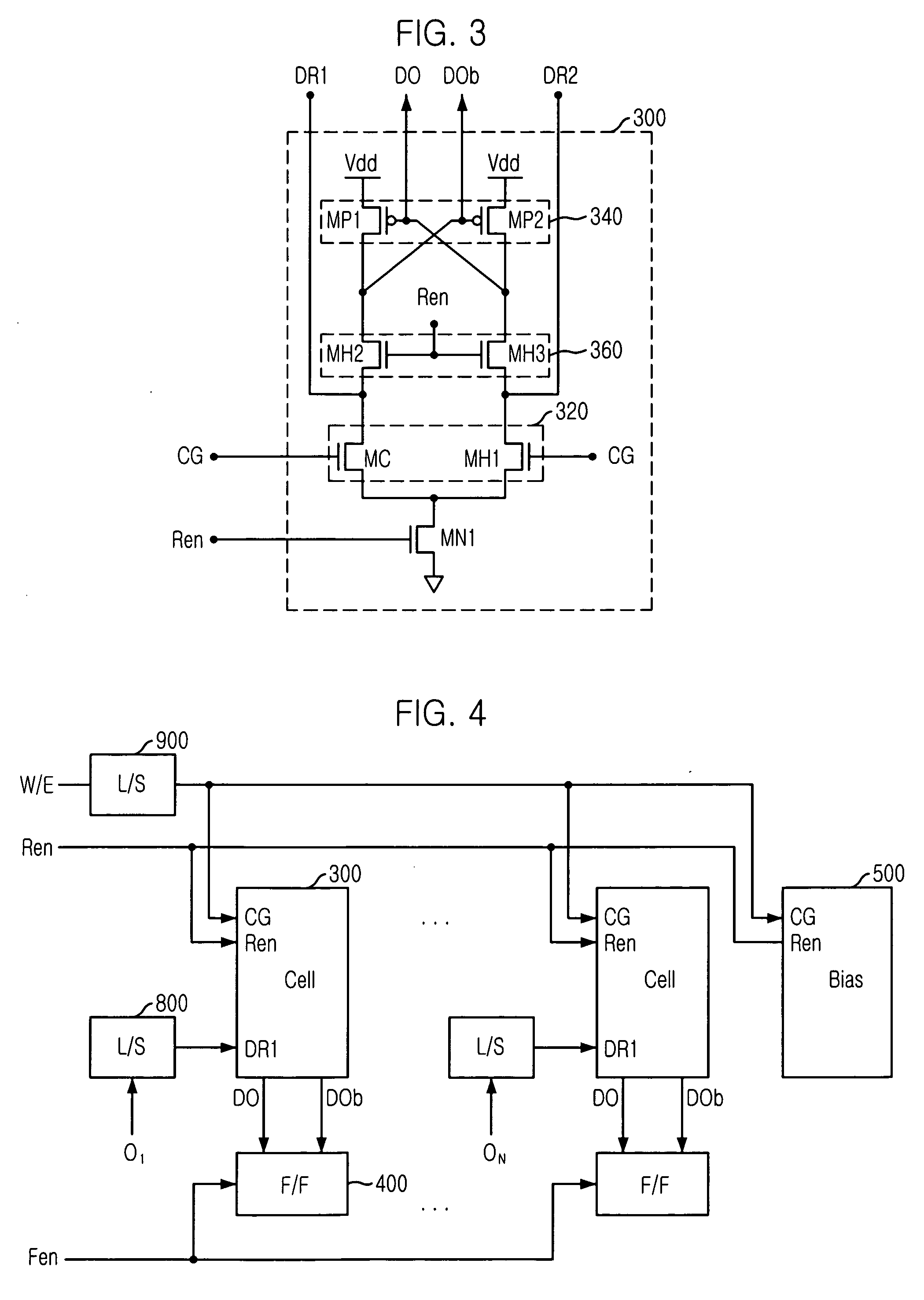
[0020] An EEPROM cell of this embodiment as shown in FIG. 3 includes a...


PUM


Abstract

The EEPROM cell includes a writing unit having a flash cell Metal Oxide Semiconductor (MOS) for receiving from outside a gate selection signal via a gate and a drain selection signal via a drain, and writing one bit data, and a high-voltage MOS whose source is connected to a source of the flash cell MOS to have a symmetrical structure and for receiving the gate selection signal via a gate, and a sensing unit having a first sensing MOS whose source is connected to a power supply voltage, gate to a drain of a second sensing MOS and drain to the drain of the flash cell MOS, and the second sensing MOS whose source is connected to the power supply voltage, gate to the drain of the first sensing MOS and drain to the drain of the high-voltage MOS.

Description

FIELD OF THE INVENTION [0001] The present invention relates to a nonvolatile memory capable of keeping data stored therein when an external power is interrupted, and more particularly, to an Electrically Erasable and Programmable Read Only Memory (EEPROM) built in a device such as a one-chip microcontroller or the like. DESCRIPTION OF RELATED ART [0002] It is well known that EEPROM is an electronic circuit that writes data as charged in a floating gate formed as dielectric in a flash cell Metal Oxide Semiconductor (MOS) transistor having the shape of MOS transistor device. This EEPROM may be implemented to use in computer systems, etc. as one auxiliary memory device by manufacturing as an independent chip device. Also, it may be implemented in an embedded shape as a storage device of data that needs to be kept when a power is cut off in a one-chip microcontroller. [0003] In universal microcontrollers or smart chips for smart card, since an embedded EEPROM having capacity of more tha...

Claims


Application Information

Patent Timeline
Patent Type & Authority Applications(United States)
IPC IPC(8): G11C19/08
CPCG11C16/08G11C8/08G11C5/14G11C7/1069G11C16/26G11C16/30
Inventor CHO, KI-SEOK
Owner MAGNACHIP SEMICONDUCTOR LTD
Why Eureka
Try Eureka