Method for forming silicon-containing materials during a photoexcitation deposition process

Inactive Publication Date: 2006-12-21
APPLIED MATERIALS INC
View PDF19 Cites 339 Cited by
  • Summary
  • Abstract
  • Description
  • Claims
  • Application Information

AI Technical Summary

Benefits of technology

[0007] Embodiments of the invention generally provide a method for depositing films using a UV source during a photoexcitation process. The films are deposited on a substrate and usually contain a material, such as silicon oxide, silicon nitride, silicon oxynitride, silicon (e.g., epitaxy, crystalline, microcrystalline, polysilicon, or amorphous), or other silicon-containing materials (e.g., SiGe, SiC, SiGeC, or doped variants thereof). The photoexcitation process may expose the substrate and/or gases to an energy beam or flux prio

Problems solved by technology

Although some thermal CVD processes for silicon-containing materials having deposition temperatures of less than 550° C. have been proposed, the processes usually lack suitable production worthiness for large scale semic

Method used


Image

  • Method for forming silicon-containing materials during a photoexcitation deposition process
  • Method for forming silicon-containing materials during a photoexcitation deposition process
  • Method for forming silicon-containing materials during a photoexcitation deposition process

Examples


Example

[0035] To facilitate understanding, identical reference numerals have been used, wherever possible, to designate identical elements that are common to the figures. It is contemplated that elements and / or process steps of one embodiment may be beneficially incorporated in other embodiments without additional recitation.

DETAILED DESCRIPTION

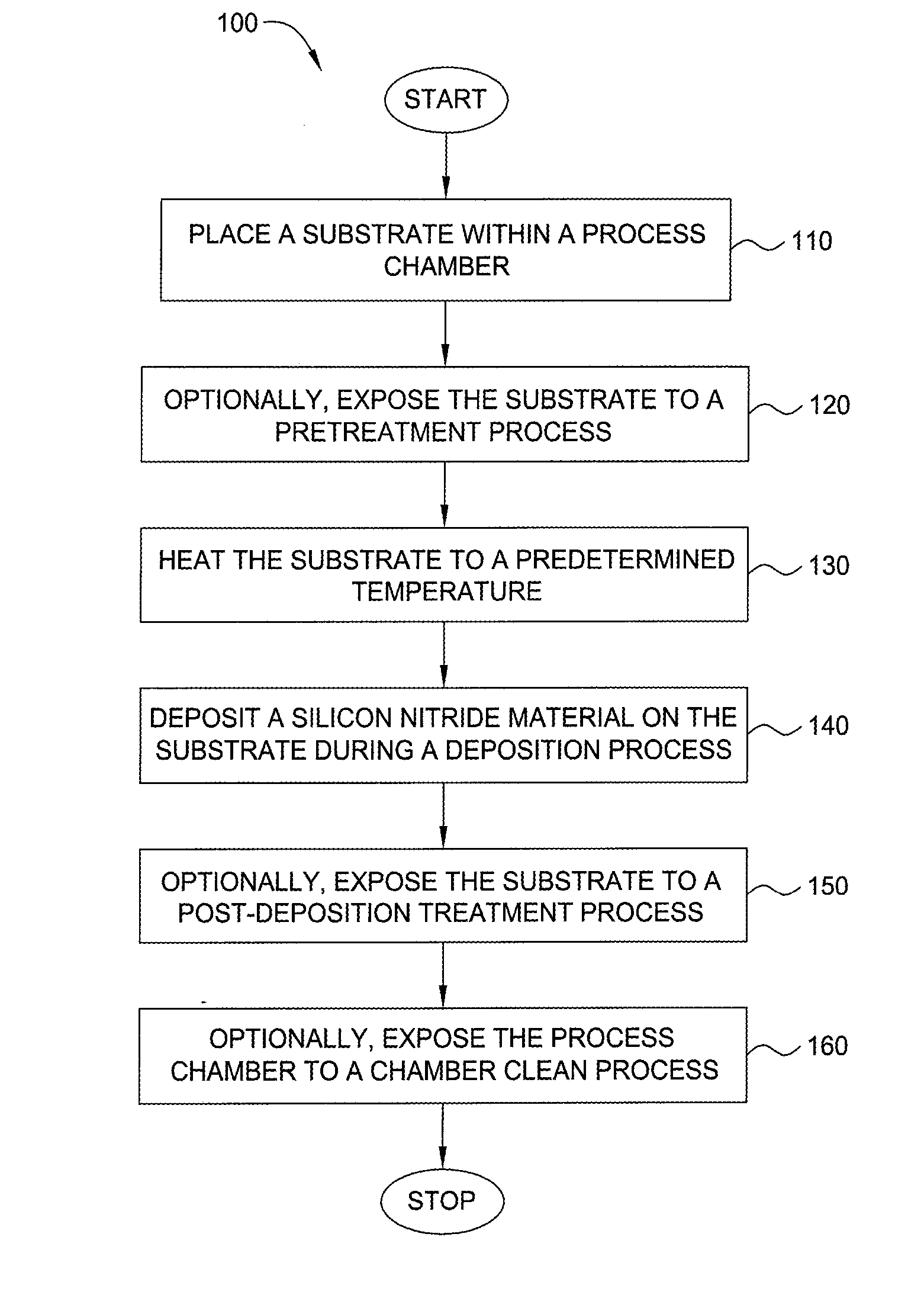
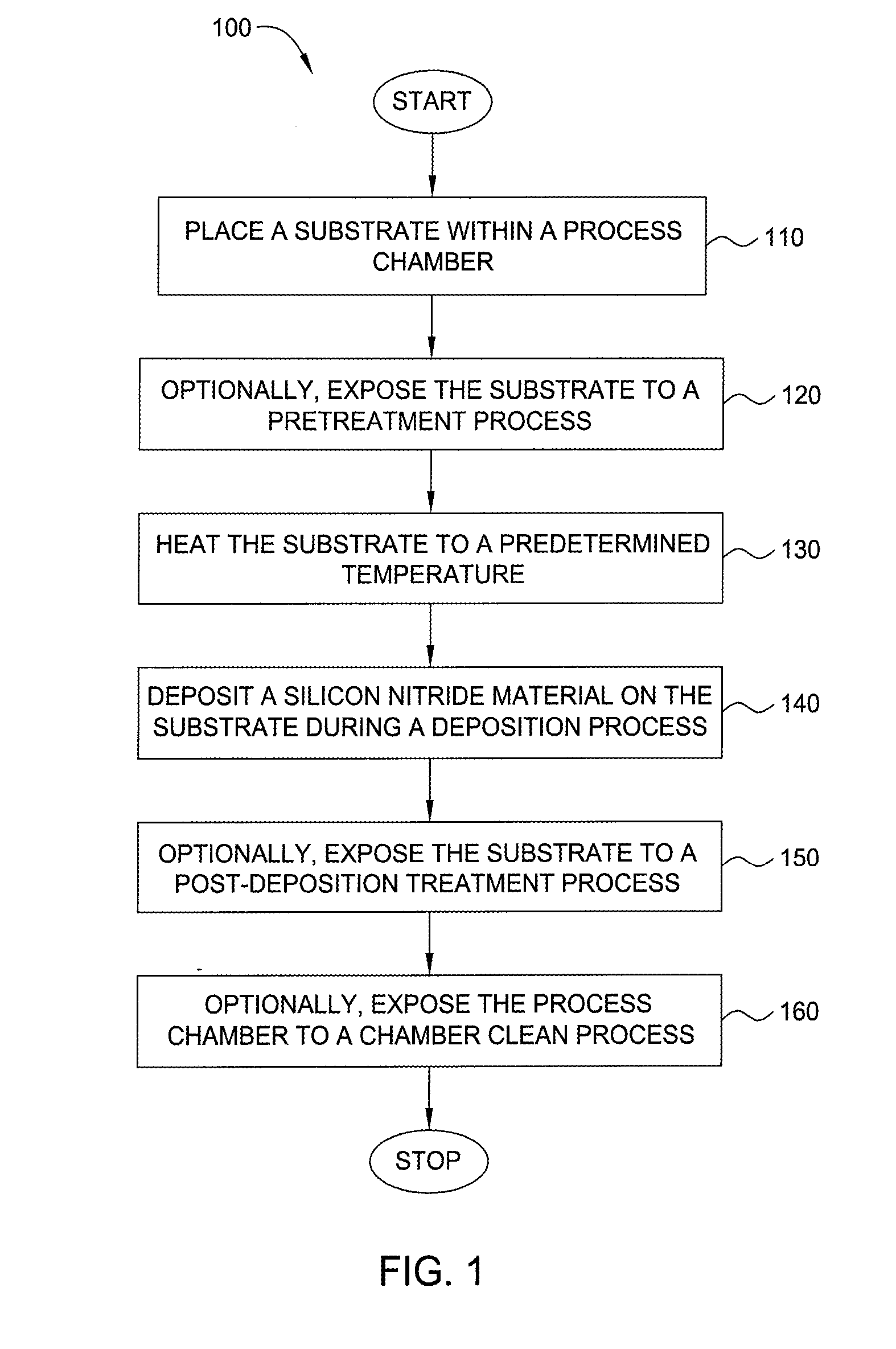
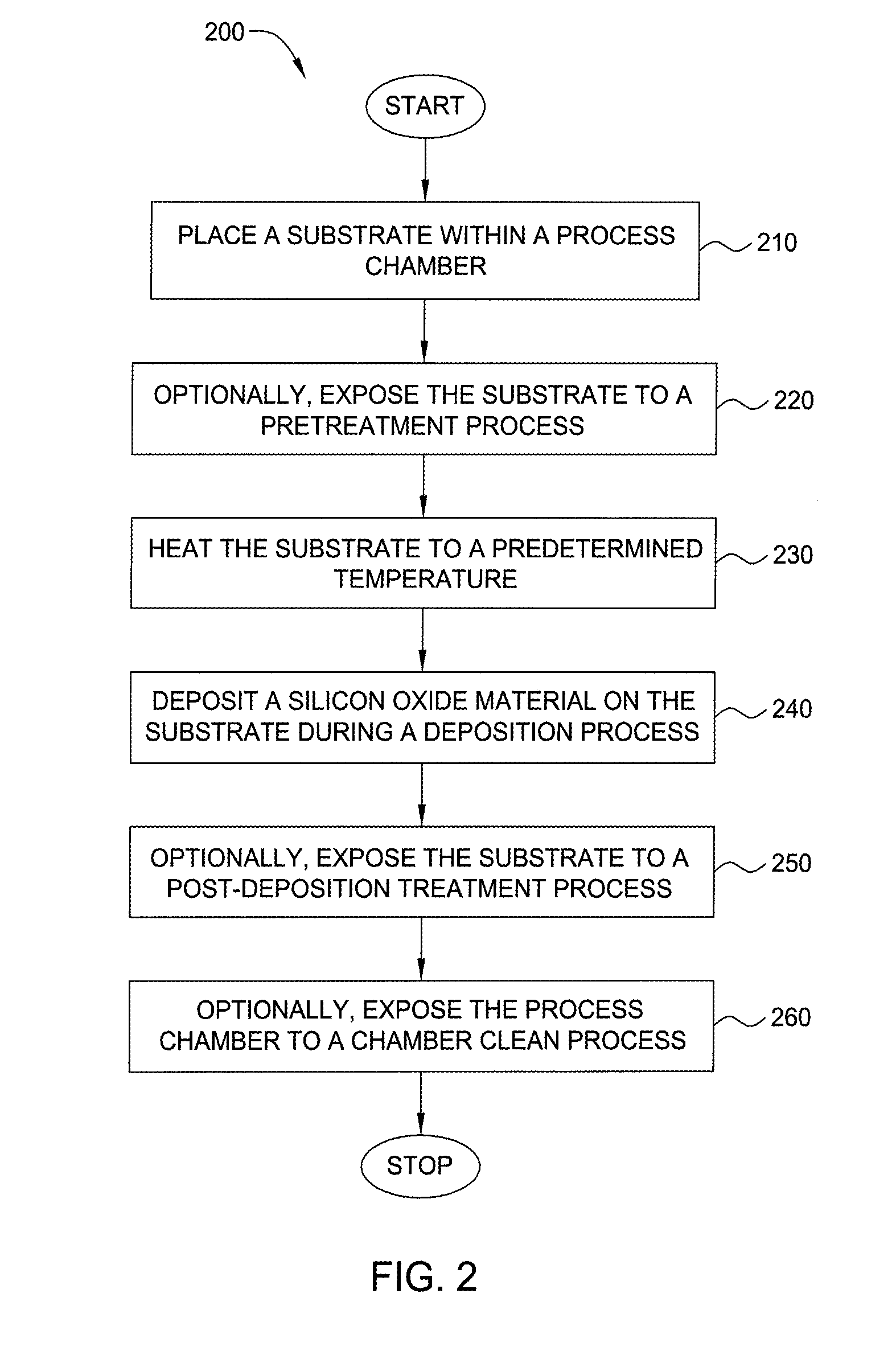
[0036] Embodiments of the invention provide a process for depositing a silicon-containing material onto a substrate. Silicon-containing materials include silicon oxide, silicon nitride, and silicon oxynitride, as well as silicon materials that may contain germanium, carbon, dopants, or combinations thereof. Many of the embodiments described herein are advantageously performed utilizing temperatures of less than about 550° C. Although some examples of the processes are described with reference to a single wafer thermal-chemical vapor deposition chamber (e.g., process chamber 1100 illustrated in FIG. 7), other processes may be beneficially practiced...


PUM

PropertyMeasurementUnit
Energyaaaaaaaaaa
Energyaaaaaaaaaa
Energyaaaaaaaaaa

Abstract

Embodiments of the invention generally provide a method for depositing films or layers using a UV source during a photoexcitation process. The films are deposited on a substrate and usually contain a material, such as silicon (e.g., epitaxy, crystalline, microcrystalline, polysilicon, or amorphous), silicon oxide, silicon nitride, silicon oxynitride, or other silicon-containing materials. The photoexcitation process may expose the substrate and/or gases to an energy beam or flux prior to, during, or subsequent a deposition process. Therefore, the photoexcitation process may be used to pre-treat or post-treat the substrate or material, to deposit the silicon-containing material, and to enhance chamber cleaning processes. Attributes of the method that are enhanced by the UV photoexcitation process include removing native oxides prior to deposition, removing volatiles from deposited films, increasing surface energy of the deposited films, increasing the excitation energy of precursors, reducing deposition time, and reducing deposition temperature.

Description

RELATED APPLICATION [0001] This application is a continuation-in-part of co-pending U.S. Ser. No. 11 / 157,567 (APPM / 007647), entitled “Methods for Treating Substrates and Films with Photoexcitation,” filed Jun. 21, 2005, and a continuation-in-part of co-pending U.S. Ser. No. 11 / 157,533 (APPM / 007647.02), entitled “Method for Silicon Based Dielectric Deposition and Clean with Photoexcitation,” filed Jun. 21, 2005, which are both herein incorporated by reference in their entirety.BACKGROUND OF THE INVENTION [0002] 1. Field of the Invention [0003] Embodiments of the invention generally relate to a method for depositing silicon-containing materials, and more particularly, embodiments of the invention relate to chemical vapor deposition processes utilizing photoexcitation techniques to deposit silicon based dielectric materials, such as silicon oxide, silicon nitride, silicon oxynitride, silicon, and other silicon materials. [0004] 2. Description of the Related Art [0005] Thermal chemical ...

Claims


Application Information

Patent Timeline
IPC IPC(8): H01L21/20
CPCC23C16/0227H01L21/02636C23C16/345C23C16/45519C23C16/45591C23C16/482C23C16/488C23C16/52C30B25/02C30B29/06H01L21/02126H01L21/0214H01L21/02164H01L21/0217H01L21/02219H01L21/02277H01L21/02301H01L21/0231H01L21/02348H01L21/3121H01L21/3143H01L21/31612H01L21/3185H01L21/02529H01L21/02532H01L21/0262H01L21/02576H01L21/02579C23C16/308
Inventor SINGH, KAUSHAL K.RANISH, JOSEPH M.
Owner APPLIED MATERIALS INC
Why Eureka
Try Eureka