Structure and method for forming laterally extending dielectric layer in a trench-gate FET

a dielectric layer and trench-gate technology, applied in the direction of semiconductor/solid-state device details, electrical apparatus, semiconductor devices, etc., can solve the problems of gate shortening and yield, gate polysilicon voiding, surface etching that is not substantial,

Active Publication Date: 2006-12-28
SEMICON COMPONENTS IND LLC
View PDF2 Cites 74 Cited by
  • Summary
  • Abstract
  • Description
  • Claims
  • Application Information

AI Technical Summary

Benefits of technology

[0007] In accordance with an embodiment of the invention, a field effect transistor (FET) is formed as follows. A trench is formed in a silicon region. An oxidation barrier layer is formed over a surface of the silicon region adjacent the trench and along the trench sidewalls and bottom. A protective layer is formed over the oxidation barrier layer ins

Problems solved by technology

This thick dielectric over the mesa surfaces causes a number of problems.
First, the thick dielectric over the mesa surfaces typically overhangs the upper trench corners, which can cause voiding in the gate polysilicon.
Additionally, removing the thick dielectric from over the mesa surfaces requires substantial etching, which can also etch the gate oxide along the upper trench sidewalls.
This can lead to gate shorts and

Method used


Image

  • Structure and method for forming laterally extending dielectric layer in a trench-gate FET
  • Structure and method for forming laterally extending dielectric layer in a trench-gate FET
  • Structure and method for forming laterally extending dielectric layer in a trench-gate FET

Examples


Embodiment Construction

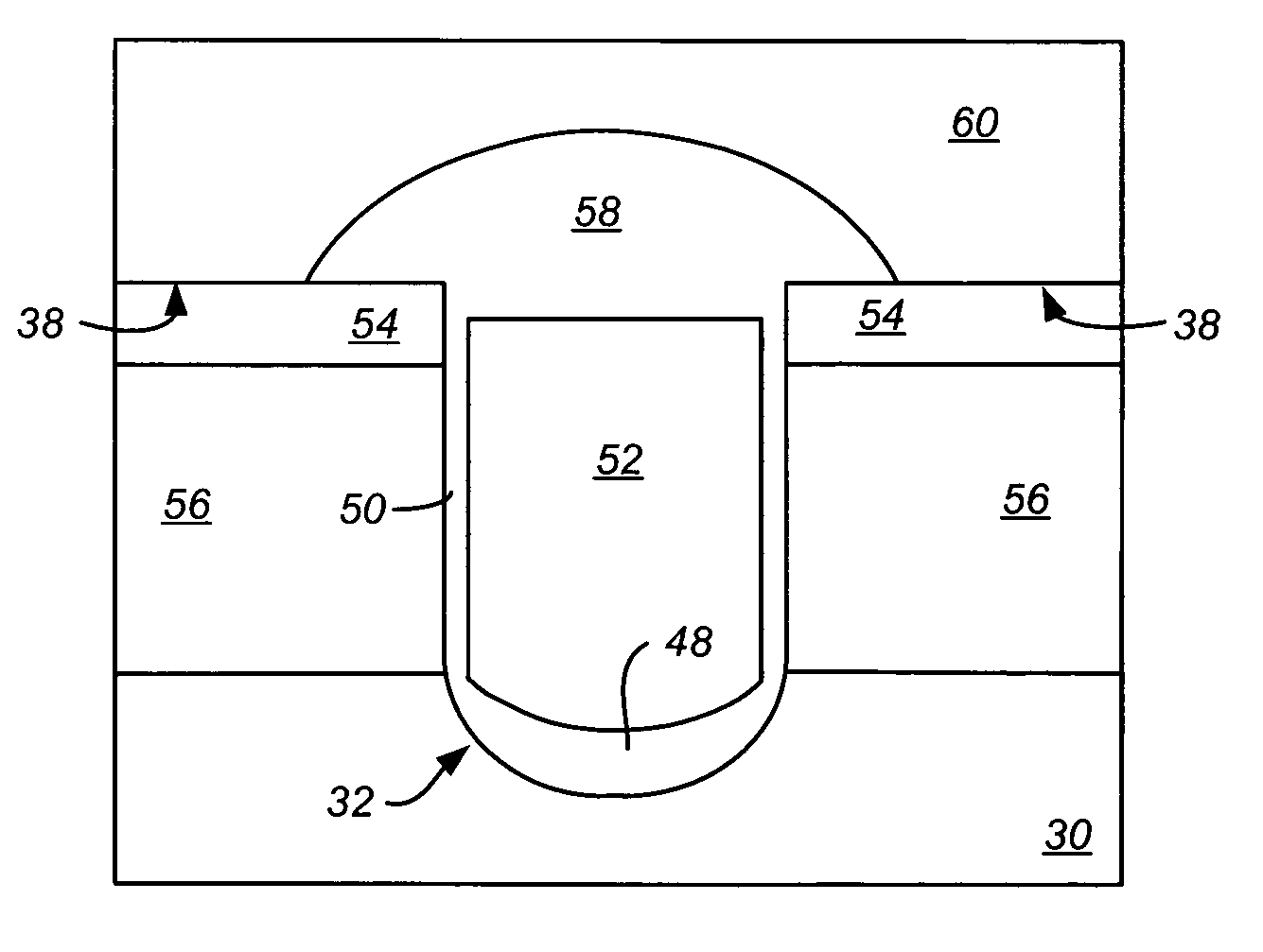
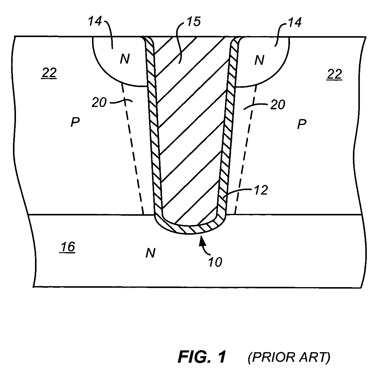
[0017] In accordance with an embodiment of the invention, a thick dielectric layer is formed along the bottom of a trench in a trench-gate FET while preventing formation of a similarly thick dielectric layer over the silicon mesa surfaces adjacent the trench by using a protective layer. The protective layer serves to protect portions of a silicon nitride layer extending over the silicon mesa surfaces during a silicon nitride etch process for removing the silicon nitride layer from along the trench bottom. In accordance with another embodiment of the invention, a similar technique is advantageously used to form the inter-poly dielectric in a shielded gate trench FET.

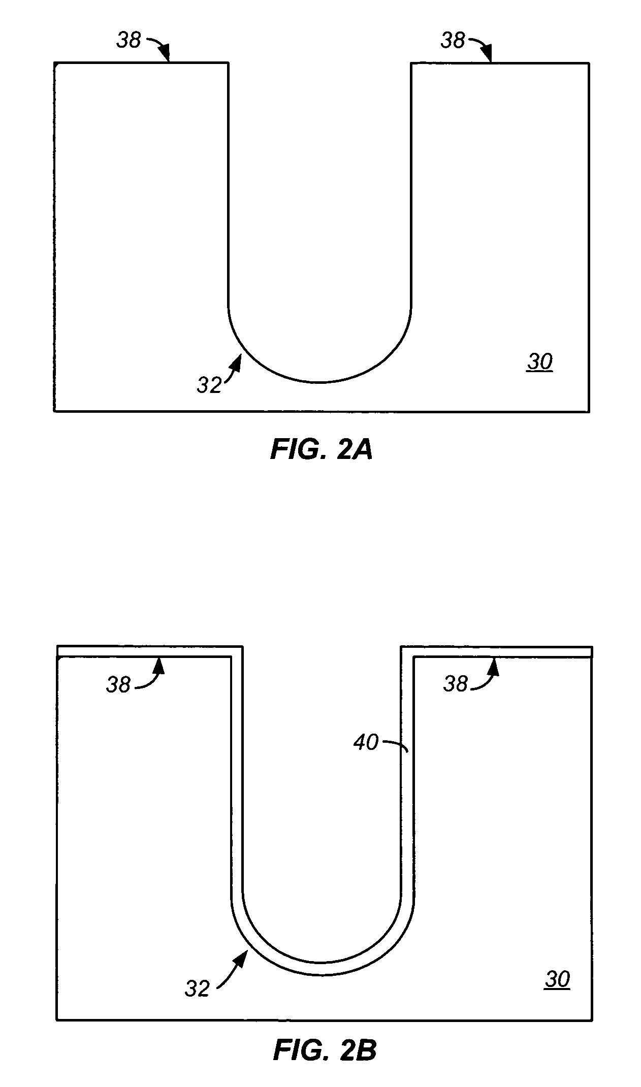
[0018]FIGS. 2A-2J show cross-section views at various steps in a manufacturing process for forming a trench-gate FET with a thick bottom dielectric, in accordance with an embodiment of the invention. The following description of the steps in the process flow is only exemplary and it should be understood that the scope of...


PUM


Abstract

A field effect transistor (FET) is formed as follows. A trench is formed in a silicon region. An oxidation barrier layer is formed over a surface of the silicon region adjacent the trench and along the trench sidewalls and bottom. A protective layer is formed over the oxidation barrier layer inside and outside the trench. The protective layer is partially removed such that a portion of the oxidation barrier layer extending at least along the trench bottom becomes exposed and portions of the oxidation barrier layer extending over the surface of the silicon region adjacent the trench remain covered by remaining portions of the protective layer.

Description

BACKGROUND OF THE INVENTION [0001] The present invention relates in general to power field effect transistors (FETs), and in particular to trench-gate FETs with improved characteristics. [0002]FIG. 1 is a simplified cross-section view of a portion of a conventional trench power metal-oxide-semiconductor field-effect transistor (MOSFET). A trench 10 is lined with a gate dielectric 12, and is filled with a conductive material 15, such as polysilicon, which forms the gate of the transistor. The trench extends from the surface of the silicon into the substrate down through a body region 22 and into a drain region 16. Body region 22 is p-type and drain region 16 is n-type. Drain region 16 may be electrically contacted through the substrate (not shown) of the transistor. Source regions 14 are formed adjacent to and on opposite sides of trench 10. An active channel region 20 is thus formed in body region 22 along the trench sidewalls between source regions 14 and drain region 16. [0003] An...

Claims


Application Information

Patent Timeline
IPC IPC(8): H01L23/58H01L21/336H01L29/78
CPCH01L29/407H01L29/42368H01L29/66734H01L2924/0002H01L2924/00
Inventor ANDREWS, JOHN TRACEY
Owner SEMICON COMPONENTS IND LLC
Why Eureka
Try Eureka