Electron emitter, charger, and charging method

a technology of electric emitters and chargers, applied in the direction of static indicating devices, instruments, corona discharges, etc., can solve the problems of accelerating the degradation of photoreceptors, requiring high voltage power supplies of about 4 to 10 kv, adversely affecting human bodies, etc., and achieve the effect of stably driving

Inactive Publication Date: 2006-12-28
SHARP KK +1
View PDF1 Cites 30 Cited by
  • Summary
  • Abstract
  • Description
  • Claims
  • Application Information

AI Technical Summary

Benefits of technology

[0010] In view of the circumstances as described above, an object of the present invention is to provide an electron ...

Problems solved by technology

This method, however, has a problem in that a high voltage power supply of about 4 to 10 kV is necessary to charge the surface of a photoreceptor.
Moreover, the discharge from the wire causes a large amount of ozone in the space between the wire and the surface of the photoreceptor, which adversely effects human bodies and also accelerates degradation of the photoreceptor.
In the roller charging scheme, however, when the surface of the photoreceptor has any minute defect (pinhole), an abnormal amount of current leak occurs in the defect portion of the surface of the photoreceptor from the conductive roller, causing the surface of the photoreceptor to be destroyed, which may adversely affect image formation.
Therefore, it wa...

Method used


Image

  • Electron emitter, charger, and charging method
  • Electron emitter, charger, and charging method
  • Electron emitter, charger, and charging method

Examples


Embodiment Construction

[0026] In the following, the embodiments of the present invention will be described. It is noted that in the figure of the specification, the same reference characters refer to the same parts or corresponding parts.

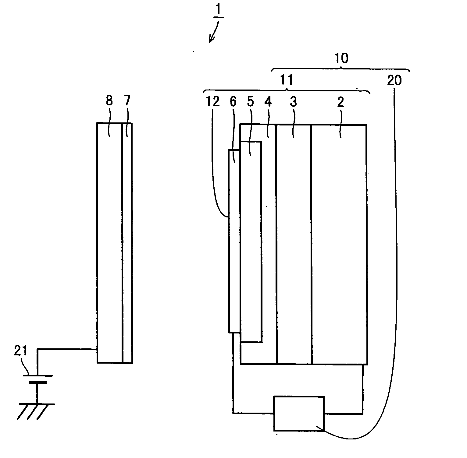
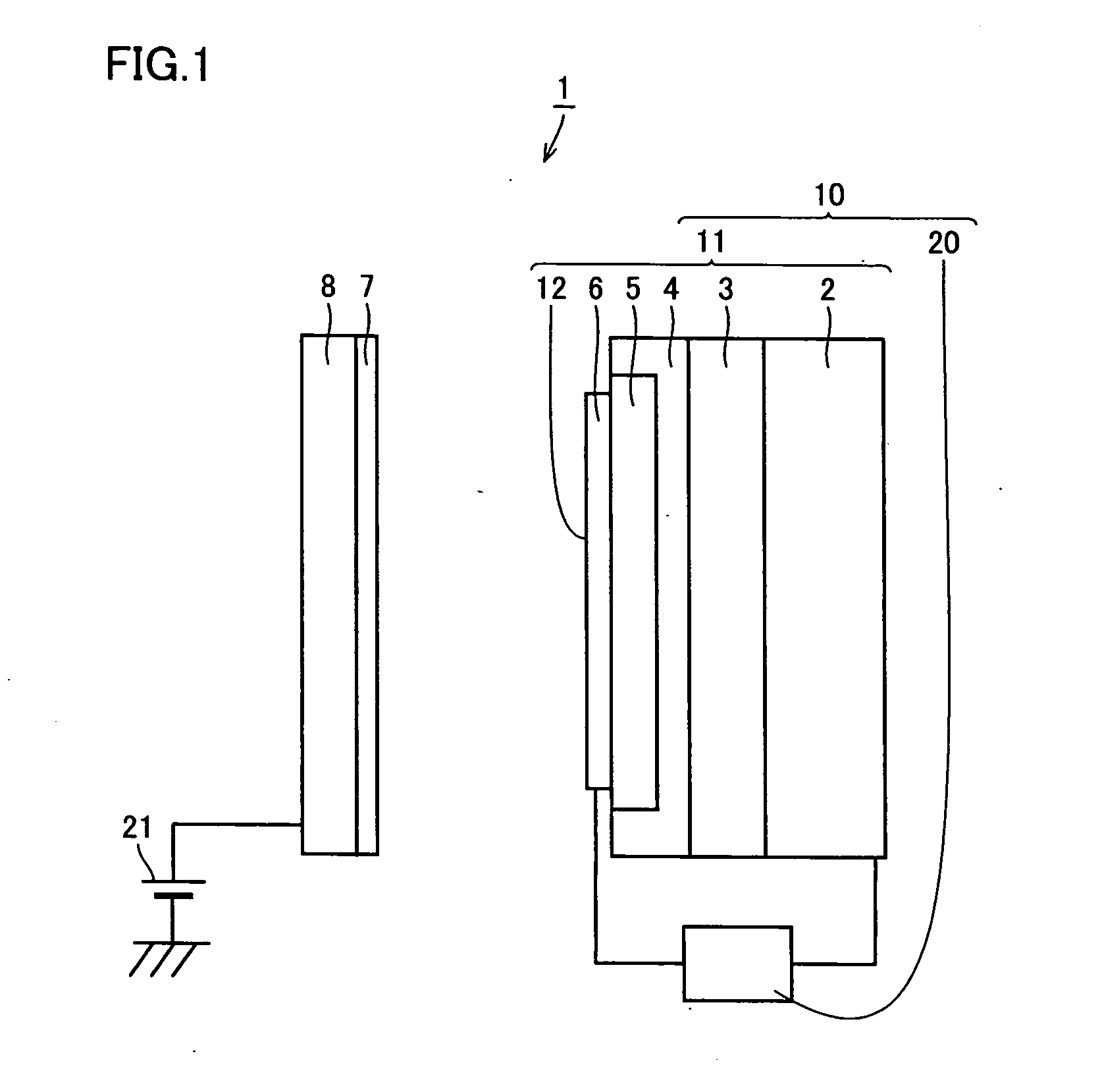
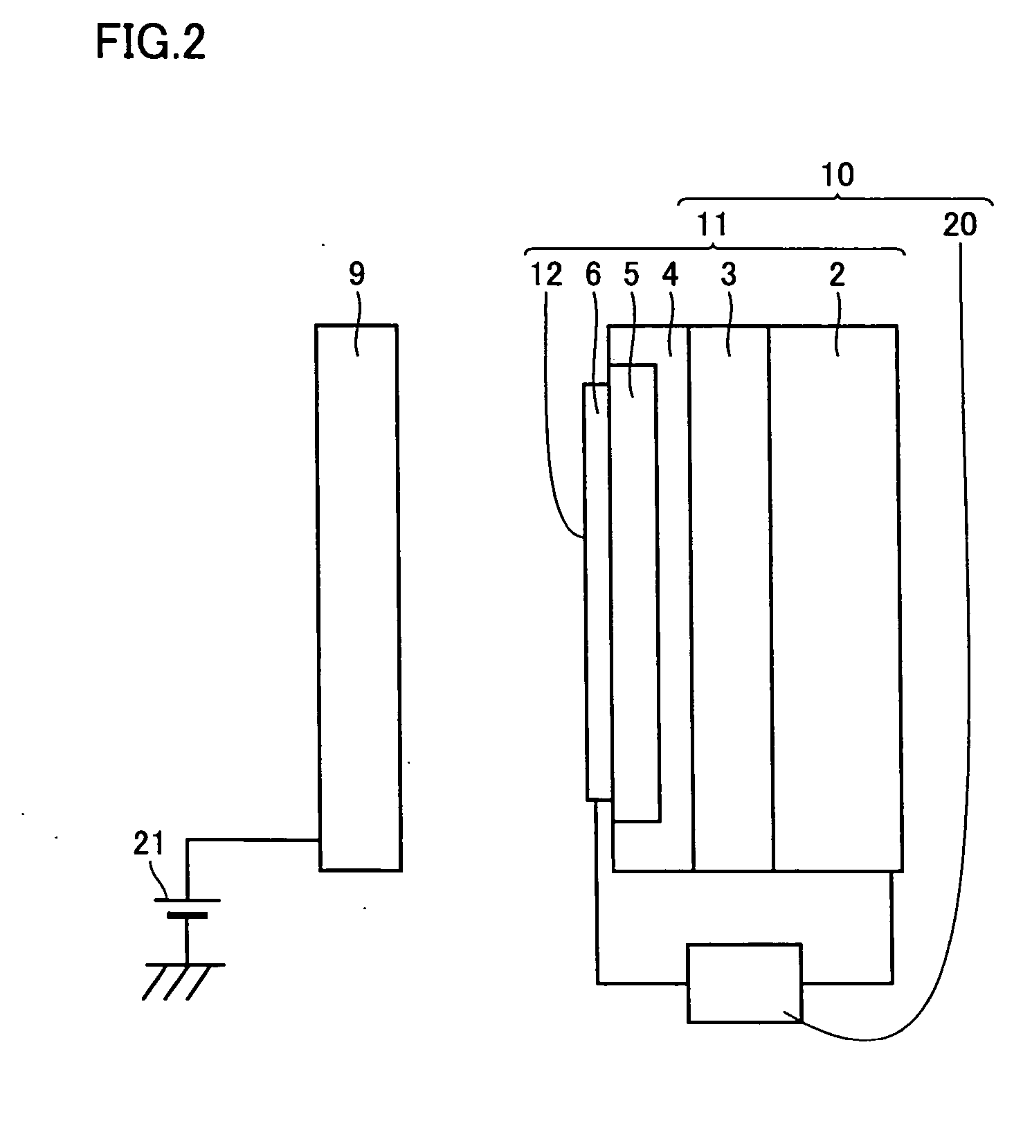
[0027]FIG. 1 shows a schematic conceptual view of a preferred exemplary charger in accordance with the present invention. This charger 1 includes an electron emitter 10 and a photoreceptor 7 as a body to be charged that is arranged opposing to and spaced apart from an electron emitting surface 12 that is a surface of an acceleration electrode 6 of electron emitter 10.

[0028] Electron emitter 10 includes an electron emitting element 11 constituted with a base electrode 2 formed of a conductive substrate, an n-type silicon layer 3 formed on base electrode 2, a non-doped thin polysilicon layer 4 formed on n-type silicon layer 3, a porous polysilicon layer 5 formed by rendering a part of polysilicon layer 4 porous, and an acceleration electrode 6 formed of a gold thin film f...


PUM


Abstract

Provided are an electron emitter continuously emitting electrons stably even in the atmosphere, a charger using the electron emitter, and a charging method using the charger. The electron emitter includes a electron emitting element consisting of a first electrode, a second electrode, and a semiconductor layer formed therebetween, and a power supply for alternately applying a positive voltage enabling electron emission and a negative voltage having a polarity opposite to the positive voltage. At least a part of the surface on the first electrode side of the semiconductor layer is formed of a porous semiconductor layer. Electrons captured in the porous semiconductor layer in the course of electron emission with application of a positive voltage disturb electron emission from the electron emitting element. Such electrons, however, are removed by application of a negative voltage.

Description

TECHNICAL FIELD [0001] The present invention relates to an electron emitter, a charger, and a charging method, and more particularly to an electron emitter, a charger, and a charging method for use in image forming devices such as electrophotographic copy machines, printers or facsimiles. BACKGROUND ART [0002] Conventionally, in an image forming device such as an electrophotographic copy machine, prior to forming an electrostatic latent image at a body to be charged such as a photoreceptor, the surface of the body to be charged is evenly charged by a variety of methods. [0003] Conventional charging methods include, for example, corona discharge. In this method, the surface of a photoreceptor is charged by discharge from an extremely fine wire. This method, however, has a problem in that a high voltage power supply of about 4 to 10 kV is necessary to charge the surface of a photoreceptor. Moreover, the discharge from the wire causes a large amount of ozone in the space between the wi...

Claims


Application Information

Patent Timeline
IPC IPC(8): G03G15/02G03G13/02H01J1/312H01J29/04H01T23/00
CPCG03G15/02
Inventor HIRAKAWA, HIROYUKIIWAMATSU, TADASHIKOSHIDA, NOBUYOSHI
Owner SHARP KK
Why Eureka
Try Eureka