Method of creating photo mask data, method of photo mask manufacturing, and method of manufacturing semiconductor device
- Summary
- Abstract
- Description
- Claims
- Application Information
AI Technical Summary
Benefits of technology
Problems solved by technology
Method used
Image

Examples
first embodiment
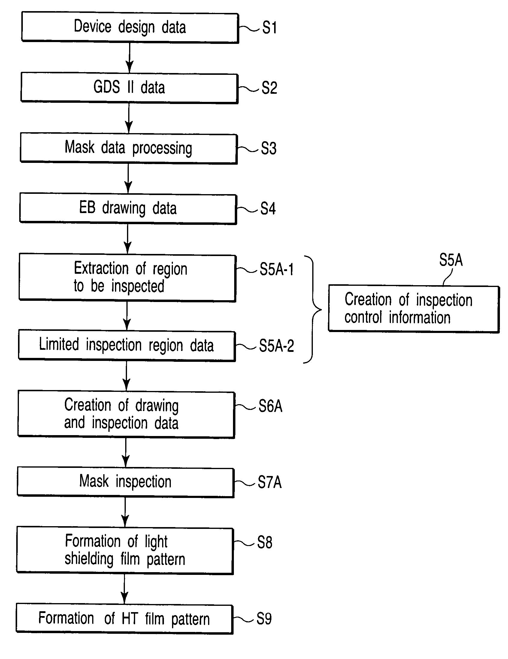
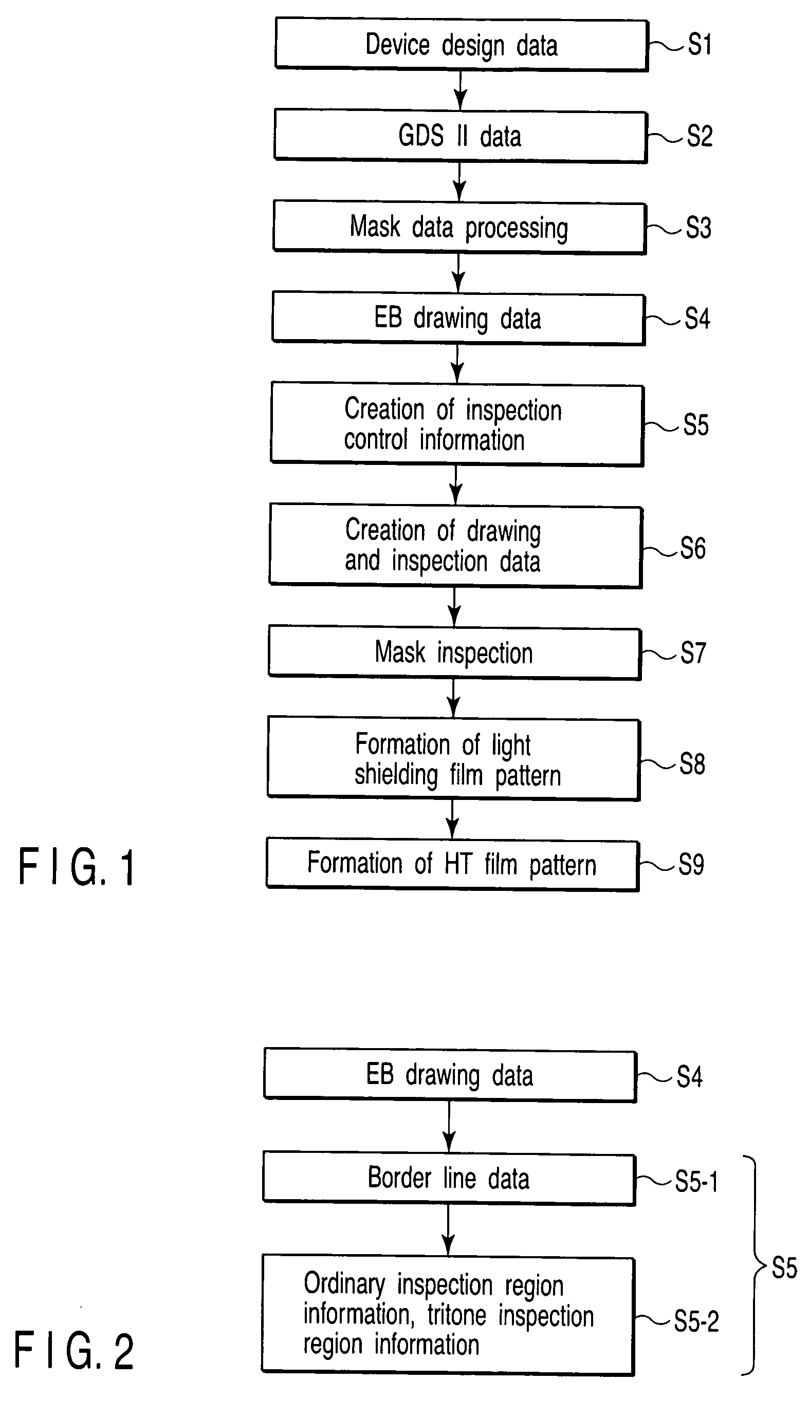
[0038]FIG. 1 is a flowchart showing a flow of a method of manufacturing a photo mask according to the first embodiment of the invention.
[0039] First, device design data of a photo mask is prepared (step S1). The device design data is created by a CAD tool.
[0040] Next, the device design data is converted into GDS II stream type data (GDS II data) (step S2). The device design data may be also converted into other data than the GDS II stream type data.
[0041] Next, mask data processing is applied to the GDS II data (step S3), and EB drawing data is created (step S4). The EB drawing data is stored in an external storage medium such as a magnetic tape or a magnetic disk.
[0042] Next, inspection control information is created by using the EB drawing data (step S5). The inspection control information is stored in the external storage medium or the like.
[0043]FIG. 2 is a flowchart showing contents of step S5.
[0044] For the sake of simplicity, herein, a part (a portion enclosed by thick ...
second embodiment
[0069]FIG. 7 is a plan view illustrating a shape defect inspection region in a photo mask according to the second embodiment of the invention.
[0070] The present embodiment is different from the first embodiment in a point that a specific region of the shape defect inspection region 2 is inspected by the shape detect inspection apparatus of die-to-database comparison system.
[0071] The shape defect inspection region 2 includes the first to sixth regions 21 to 26. The first and sixth regions 21, 26 require die-to-database comparison system inspection, and the second to fifth regions 22 to 25 do not require die-to-database comparison system inspection.
[0072]FIG. 8 is a flowchart showing a flow of a method of manufacturing a photo mask according to the present embodiment. Same parts corresponding to those in FIG. 1 are identified with same reference numerals, and specific description is omitted (same in the other embodiments).
[0073] According to the method of manufacturing the photo ...
third embodiment
[0090]FIG. 9 is a plan view illustrating a shape defect inspection region in a photo mask according to the third embodiment of the invention.
[0091] The present embodiment is different from the first embodiment in a point that a region excluding part of a region of a shape defect inspection region 2 (non-inspection region) is inspected by a shape detect inspection apparatus of die-to-database comparison system.
[0092] Specifically, when location of a pattern including noise source or a pattern including false defect source such as a fine OPC pattern existing in the shape defect inspection region 2, has been known preliminarily, the region including such patterns can be excluded from the inspection region before inspection.
[0093] In the case of the shape defect inspection region 2 in FIG. 9, regions 81, 82 out of the regions 22, 26 are regions excluded from the inspection regions. That is, the regions 81, 82 are regions including a false defect causing pattern or a noise causing pat...
PUM
 Abstract
Description
Claims
Application Information
 - R&D
- Intellectual Property
- Life Sciences
- Materials
- Tech Scout
- Unparalleled Data Quality
- Higher Quality Content
- 60% Fewer Hallucinations
Browse by: Latest US Patents, China's latest patents, Technical Efficacy Thesaurus, Application Domain, Technology Topic, Popular Technical Reports.
© 2025 PatSnap. All rights reserved.Legal|Privacy policy|Modern Slavery Act Transparency Statement|Sitemap|About US| Contact US: help@patsnap.com