Method for growth and optimization of heterojunction bipolar transistor film stacks by remote injection

a technology of heterojunction bipolar transistor and film stack, which is applied in the direction of basic electric elements, electrical apparatus, semiconductor devices, etc., can solve the problems of reducing the maximum operating, reducing process control, and direct injection necessitating an increase in process complexity, so as to prevent the outdiffusion of boron and eliminate or minimize the deleterious effects

Inactive Publication Date: 2006-12-28
ATMEL CORP
View PDF62 Cites 26 Cited by
  • Summary
  • Abstract
  • Description
  • Claims
  • Application Information

AI Technical Summary

Benefits of technology

[0014] The present invention is also a heterojunction bipolar transistor fabricated by methods presented herein. An exemplary HBT includes substantially-silicon collector and emitter layers with a heavily-doped base layer made substantially of boron-doped silicon-germanium. The base layer is disposed between the emitter layer and the collector layer. The base layer incorporates the remotely-injected carbon in a level of between about 0.1% and 5%, to prevent the outdiffusion of boron and additionally eliminates or minimizes the deleterious effects of the prior art.

Problems solved by technology

However, such direct injection techniques frequently lead to deleterious effects such as increased base resistance (likely due to increased impurity scattering and / or a reduction in an electrically active dopant) causing a reduction in a maximum operating frequency, updiffusion of oxygen into the SiGe base region (oxygen may decrease minority carrier lifetimes and increase base current), and outdiffusion of germanium (affecting a shape and, consequently, a function of emitter-base and collector-base energy band offsets).
Additionally, direct injection necessitates an increased process complexity, leading to reduced process control, by requiring, for example, a methyl silane injection (or another carbon precursor) to be injected concurrently with diborane (or another boron precursor), silane (or another silicon precursor), and a hydrogen carrier gas.
Such a complex precursor flow results in complex and frequently competing reactions coupled with an increase in process recipe complexity due to, inter alia, additional flow and temperature monitoring requirements.
The thin, heavily doped base maintains a low base-spreading resistance, leading to a high maximum oscillation frequency.

Method used


Image

  • Method for growth and optimization of heterojunction bipolar transistor film stacks by remote injection
  • Method for growth and optimization of heterojunction bipolar transistor film stacks by remote injection
  • Method for growth and optimization of heterojunction bipolar transistor film stacks by remote injection

Examples


Embodiment Construction

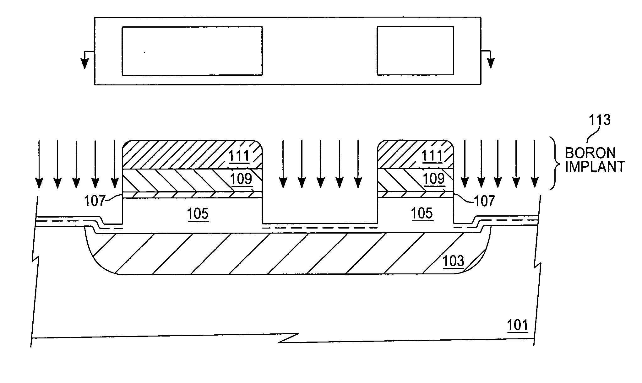
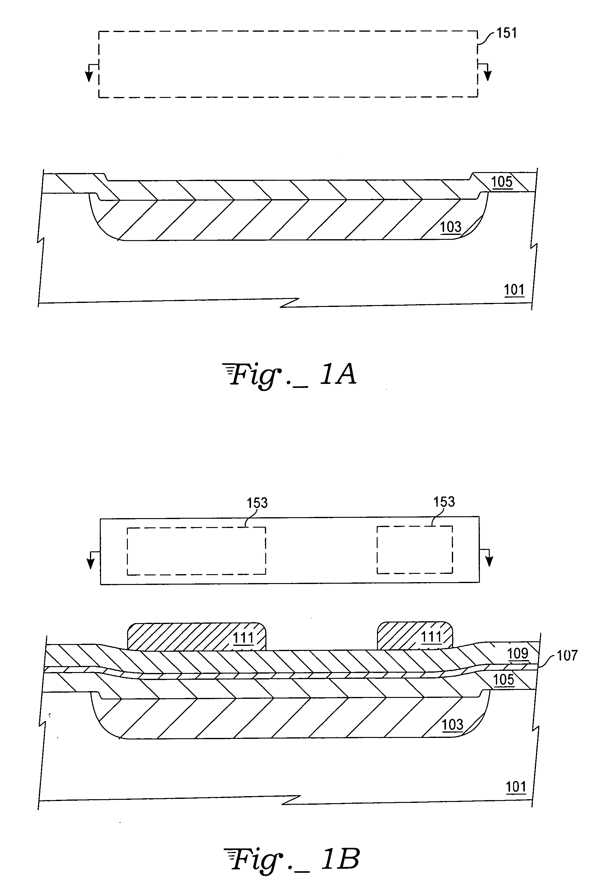
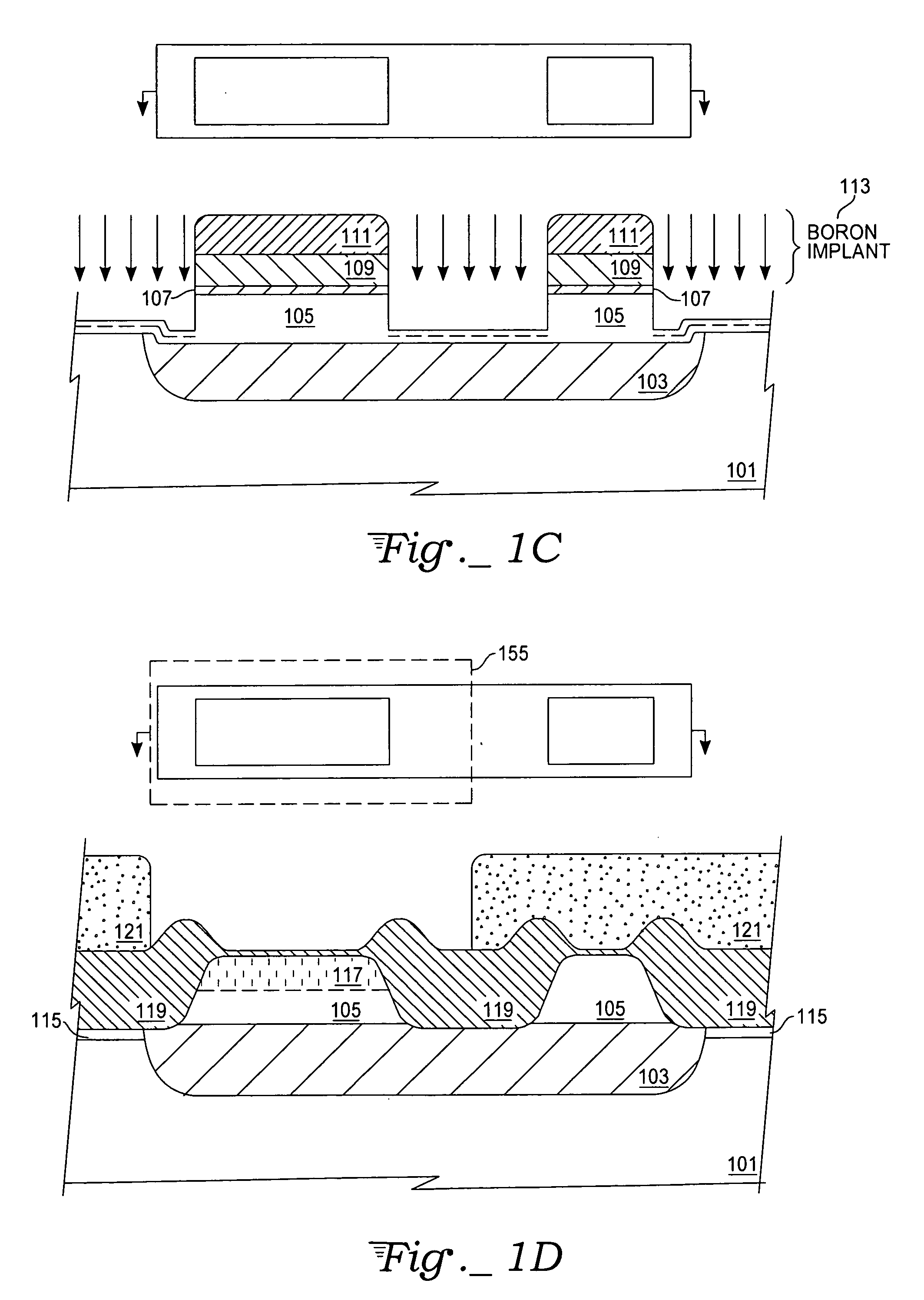
[0018] With reference to FIGS. 1A-1F, overall exemplary process steps of a typical HBT device are detailed to illustrate remote injection techniques of the present invention. For simplicity, a single bipolar device region is shown in the drawings. Other electronic device regions (e.g., CMOS transistors) as well as digital logic circuitry may be formed adjacent to the bipolar device region depicted in the drawings. Further, one skilled in the art of bipolar transistor fabrication will realize that the exemplary process steps described herein may be substantially different from other known bipolar processes but, nonetheless, the remote injection techniques described are readily amenable to other processes.

[0019]FIG. 1A is an early-stage cross-section of an npn HBT device and includes a substrate 101, an n+ buried layer 103, and a deposited n-epitaxial layer 105. In a specific exemplary embodiment, the substrate 101 is a p-type silicon wafer and the n-epitaxial layer is comprised of d...


PUM

PropertyMeasurementUnit
thicknessaaaaaaaaaa
thicknessaaaaaaaaaa
temperaturesaaaaaaaaaa

Abstract

A method, and a resulting device, for fabricating a heterojunction bipolar transistor (HBT). HBT devices have a high transconductance typical of bipolar devices and are additionally capable of high-power operation. To achieve the aforementioned characteristics, HBT devices are generally of the npn type, preferably with a thin, heavily doped base. The thin, heavily doped base maintains a low base-spreading resistance, leading to a high maximum oscillation frequency. In order to maintain a high doping concentration while minimizing outdiffusion of the dopant material, carbon is remotely doped into the base region. Details of the carbon dopant techniques and procedures are described with respect to fabrication of an exemplary HBT device.

Description

TECHNICAL FIELD [0001] The invention generally relates to methods of fabrication of integrated circuits (ICs). More specifically, the invention is a method of fabricating heterojunction bipolar transistors utilizing elemental or compound semiconducting materials and resulting devices produced by such methods. BACKGROUND ART [0002] Bipolar transistors are an advantageous choice over field effect transistors due to their superior current-drive performance, high frequency response characteristics, and power-handling ability. Consequently, research and development of bipolar transistors using not only silicon (or other group IV materials) but also compound semiconductors (e.g., compounds of elements, especially elements from periodic table groups III-V and II-VI) has seen increased activity in recent years. [0003] Significant growth in both high-frequency wired and wireless markets has introduced new opportunities where compound semiconductors such as SiGe have unique advantages over bu...

Claims


Application Information

Patent Timeline
Patent Type & Authority Applications(United States)
IPC IPC(8): H01L21/331
CPCH01L29/7378H01L29/66242
Inventor ENICKS, DARWIN G.CARVER, DAMIAN A.
Owner ATMEL CORP
Why Eureka
Try Eureka