Method for producing single crystal and single crystal

a single crystal and production method technology, applied in the direction of polycrystalline material growth, crystal growth process, polycrystalline material growth, etc., can solve the problems of deterioration of electric property like oxide dielectric breakdown voltage characteristics, unknown desired defect-free region, and difficulty in obtaining efficiently a single crystal with high quality

Active Publication Date: 2007-01-04
SHIN-ETSU HANDOTAI CO LTD
View PDF41 Cites 3 Cited by
  • Summary
  • Abstract
  • Description
  • Claims
  • Application Information

AI Technical Summary

Benefits of technology

[0016] The present invention was accomplished in view of the aforementioned circumstances, and its object is to provide a method for producing a single crystal in which when a single crystal is pulled with con

Problems solved by technology

Because devices have come to be finer, a problem of Grown-in defects introduced during growth of a crystal has become more important.
And it has been found that the Cu deposition defect region causes deterioration of electric property like oxide dielectric breakdown voltage characteristics.
Especially, there are such a case that, although a furnace structure (hot zone: HZ) is prepared so that a temperature gradient G at the solid-liquid interface becomes large in order to incre

Method used


Image

  • Method for producing single crystal and single crystal
  • Method for producing single crystal and single crystal
  • Method for producing single crystal and single crystal

Examples


example 1

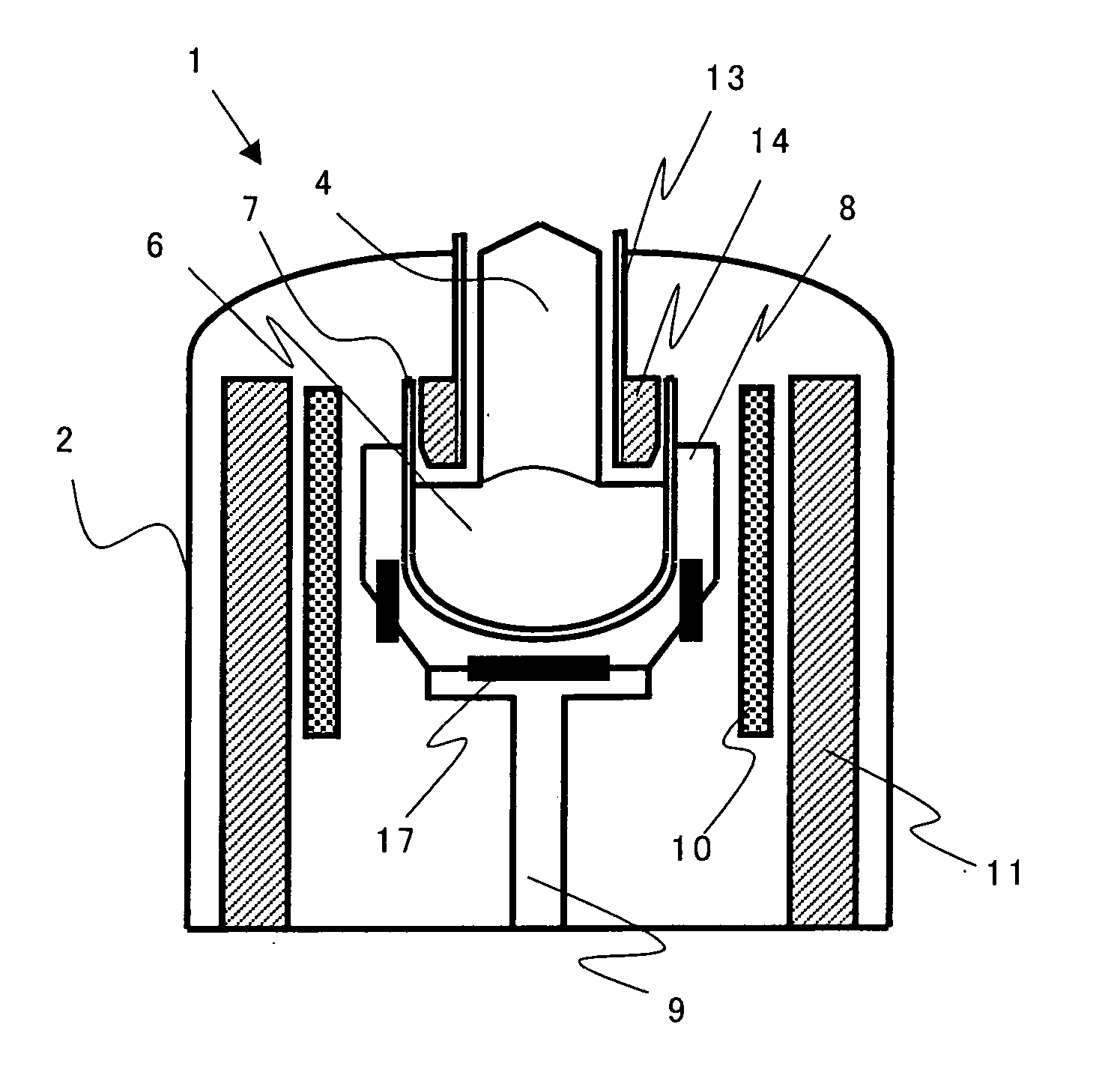
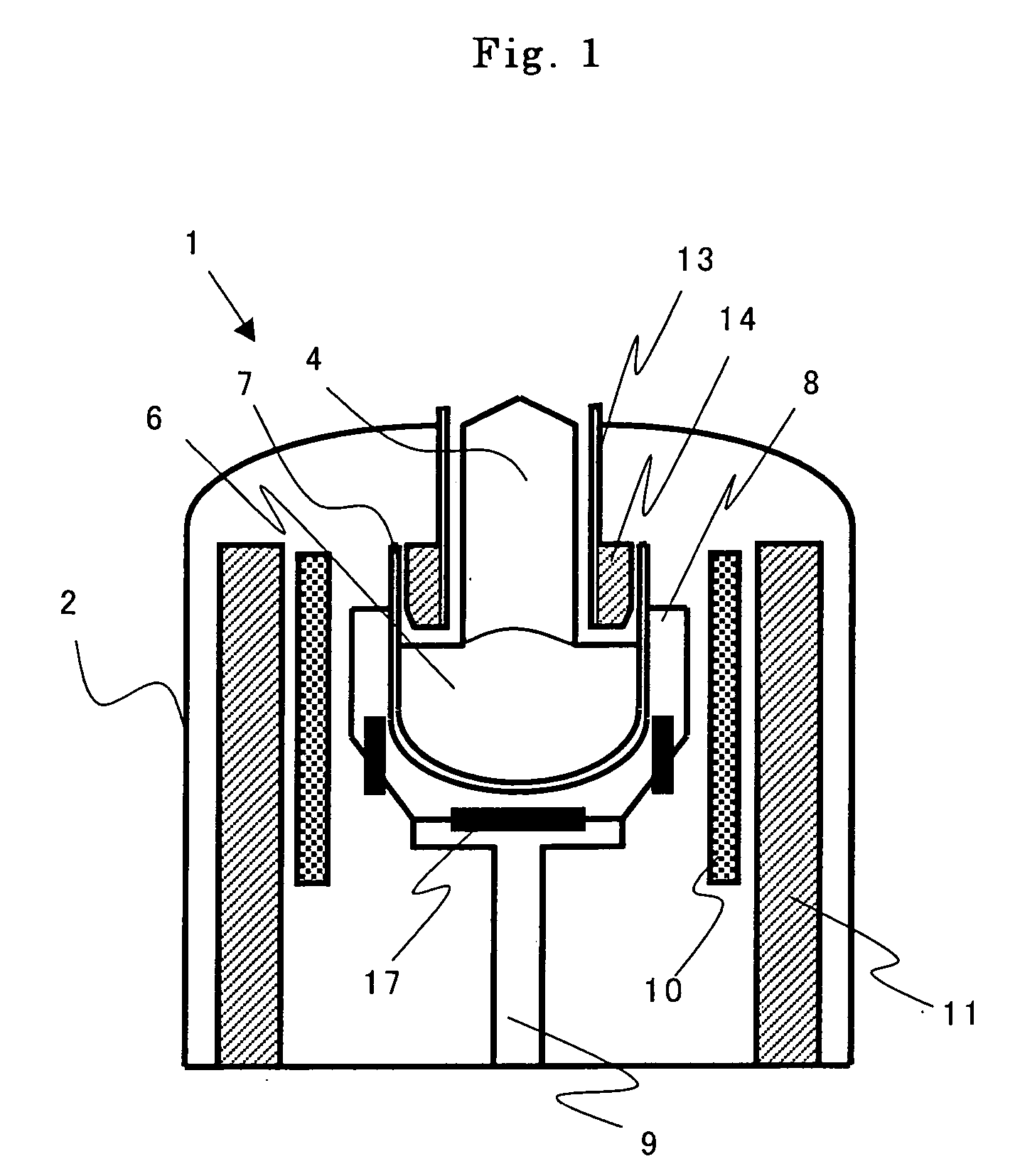
[0066] Using an apparatus for producing a single crystal, which has the crucible with a diameter of 600 mm (24 inches), as shown in FIG. 1, a silicon single crystal with a diameter of 8 inches (200 mm) was pulled so that the whole plane of the crystal would be N region without Cu deposition defect region.

[0067] For that purpose, firstly, heat insulating materials were provided below and at the side of the crucible, the highest temperature Tmax (° C.) at an interface between the crucible and a raw material melt was set at 1514 (° C.). In order to produce a single crystal including N region without Cu deposition defect region when the Tmax (° C.) is set above, a range of a value of V / G (mm2 / K·min) should be in the range from 0.21 to 0.25 (from −0.000724×1514+1.31 to −0.000724×1514+1.35) (See FIG. 3(c)). Accordingly, the range from 0.22 to 0.24 was selected as a range of a value of V / G (mm2 / K·min) to unfailingly pull a single crystal the whole plane of which is occupied by N region wi...

example 2

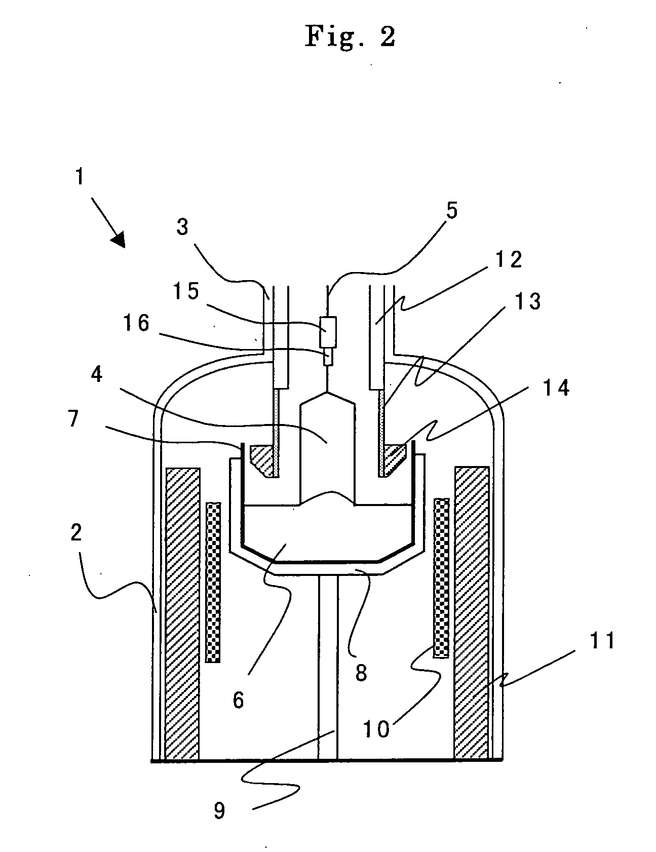
[0069] Using the same apparatus for producing a single crystal as Example 1, a silicon single crystal with a diameter of 8 inches (200 mm) was pulled so that the whole plane of the crystal would be N region without Cu deposition defect region. However, heat insulating materials which can change a highest temperature Tmax (° C.) at an interface between a crucible and a raw material melt were not provided.

[0070] In the apparatus for producing a single crystal, the highest temperature Tmax (° C.) at an interface between a crucible and a raw material melt was 1560 (° C.). In order to produce a single crystal including N region without Cu deposition defect region with the Tmax (° C.), a range of a value of V / G (mm2 / K·min) should be in the range from 0.18 to 0.22 (from −0.000724×1560+1.31 to −0.000724×1560+1.35). Accordingly, the range from 0.19 to 0.21 was selected as a range of a value of V / G (mm2 / K·min) to unfailingly pull a single crystal the whole plane of which is occupied by N reg...

example 3

[0072] Using a different apparatus for producing a single crystal, which has a crucible with a diameter of 750 mm (30 inches), from that of Example 1 and 2, a silicon single crystal with a diameter of 8 inches (200 mm) was pulled so that the whole plane of the crystal would be N region without Cu deposition defect region.

[0073] In the apparatus for producing a single crystal, the highest temperature Tmax (° C.) at an interface between the crucible and a raw material melt was 1600° C. In order to produce a single crystal including N region without Cu deposition defect region with the Tmax (° C.), a range of a value of V / G (mm2 / K·min) should be in the range from 0.15 to 0.19 (from −0.000724×1600+1.31 to −0.000724×1600+1.35). Accordingly, the range from 0.16 to 0.18 was selected as a range of a value of V / G (mm2 / K·min) to unfailingly pull a single crystal the whole plane of which is occupied by N region without Cu deposition defect region. Next, a single crystal was pulled with contro...


PUM


Abstract

The present invention is a method for producing a single crystal by Czochralski method with pulling a seed crystal from a raw material melt, wherein when a pulling rate of pulling a single crystal is defined as V (mm/min), a temperature gradient at a solid-liquid interface is defined as G (K/mm) and a highest temperature at an interface between a crucible and a raw material melt is defined as Tmax (° C.), at least, a range of a value of V/G (mm2/K·min) including a desired defect region and/or a desired defect-free region is determined according to the Tmax (° C.), and the single crystal is pulled with controlling a value of V/G (mm2/K·min) within the determined range. There can be provided a method for producing a single crystal in which when a single crystal is pulled with controlling a value of V/G, a value of V/G including a desired defect region and/or a desired defect-free region can be determined more precisely and a single crystal with desired quality can be more surely pulled.

Description

TECHNICAL FIELD [0001] The present invention relates to a method for producing a single crystal by Czochralski Method, more particularly, to a method for producing a single crystal occupied by a desired defect region and / or a desired defect-free region. BACKGROUND TECHNOLOGY [0002] A single crystal used as a substrate of semiconductor devices is, for example, a silicon single crystal. It is mainly produced by Czochralski Method (referred to as CZ method for short hereafter). [0003] When producing a single crystal by CZ method, for example, an apparatus 1 for producing a single crystal as shown in FIG. 2 is used to produce the single crystal. This apparatus 1 for producing a single crystal has a member for containing and melting a polycrystalline material such as silicon, heat insulating members to insulate heat, and etc. They are installed in a main chamber 2. A pulling chamber 3 extending upwardly is continuously provided from a ceiling portion of the main chamber 2, and a mechanis...

Claims


Application Information

Patent Timeline
IPC IPC(8): C30B15/00C30B21/06C30B27/02C30B28/10C30B30/04C30B15/20C30B29/06
CPCC30B15/203Y10S117/911C30B29/06C30B15/20
Inventor IIDA, MAKOTO
Owner SHIN-ETSU HANDOTAI CO LTD
Why Eureka
Try Eureka