Substrate for device bonding, device bonded substrate, and method for producing same

Inactive Publication Date: 2007-01-04
TOKUYAMA CORP
View PDF15 Cites 15 Cited by
  • Summary
  • Abstract
  • Description
  • Claims
  • Application Information

AI Technical Summary

Benefits of technology

[0044] According to the substrate for device bonding of the invention, it becomes possible to bond semiconductor devices without using a Sn—Pb eutectic solder that is considered to have a fear of harmfulness. Further, since the solder used in the substrate for device bonding of the invention has a melting point of almost the same level as that of a Sn—Pb eutectic solder, a conventional reflow process using a Sn—Pb eutectic solder can be adopted without largely modifying the process, and it becomes possible to solder semiconductor devices with high bond strength at

Problems solved by technology

On the other hand, so-called Pb-free solders containing no lead component h

Method used


Image

  • Substrate for device bonding, device bonded substrate, and method for producing same
  • Substrate for device bonding, device bonded substrate, and method for producing same
  • Substrate for device bonding, device bonded substrate, and method for producing same

Examples


example 1

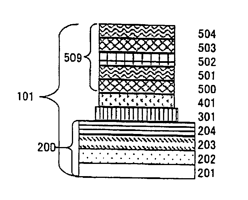
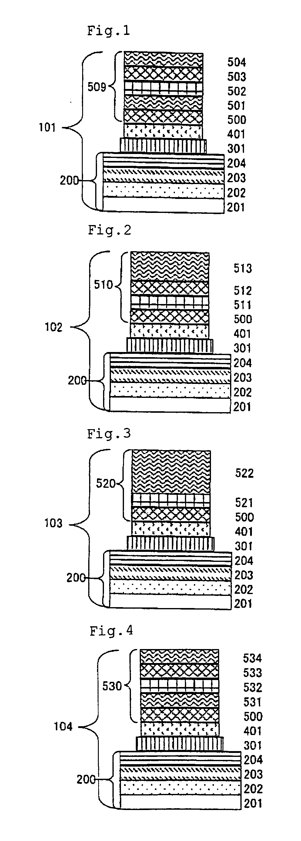
[0080] A substrate for device bonding having such a structure as is shown in FIG. 1 was prepared in the following manner. FIG. 1 is a sectional view of a typical substrate for device bonding 101 of the present invention. The substrate 200 consists of an aluminum nitride sintered substrate 201, a first undercoating layer 202 containing Ti as a main component, a second undercoating layer 203 containing platinum as a main component and a gold electrode layer 204 laminated in this order. The substrate for device bonding 101 has a structure wherein on a gold electrode layer 204 of the substrate 200, a solder flow-out preventing Pt layer 301, a bonding layer 401 containing Ti as a main component and a solder layer 509 are laminated, wherein the solder layer 509 consists of a first Ag layer 500, a first Au10-Sn layer 501, a Bi layer 502, a second Ag layer 503 and a second Au10-Sn layer 504 laminated in this order.

[0081] First, on a surface of an aluminum nitride sintered substrate (50.8 m...

example 2

[0086] A substrate for device bonding was prepared in the same manner as in Example 1, except that the structure of the solder layer 510 was changed to that wherein on the first Ag layer 500 having a thickness of 1.5 μm, a Bi layer 511 having a thickness of 0.33 μm, a second Ag layer 512 having a thickness of 0.2 μm and a first Au10-Sn layer 513 having a thickness of 3.47 μm were laminated in this order, as shown in FIG. 2. Using the substrate for device bonding, a device bonded substrate (No. 9) was prepared at the same bonding temperature as in Example 1. Similarly, 10 device bonded substrates were prepared, and the surface roughness and the bond strength of the device bonded substrates were measured in the same manner as in Example 1. As a result, Ra was 0.044 μm, Rmax was 0.390 μm, the mean bond strength was 3.1 kgf / mm2, and the modes of peeling were mainly “inside semiconductor device”. Further, substrates for device bonding No. 10 to No. 15 of the invention were prepared by ch...

example 3

[0087] A device bonded substrate (No. 16) was prepared in the same manner as in Example 1, except that the structure of the solder layer 520 was changed to that wherein on the first Ag layer 500 having a thickness of 1.5 μm, a Bi layer 521 having a thickness of 0.33 μm and a first Au10-Sn layer 522 having a thickness of 3.67 μm were laminated in this order, as shown in FIG. 3. Similarly, 10 device bonded substrates were prepared, and the surface roughness and the bond strength of the device bonded substrates were measured in the same manner as in Example 1. As a result, Ra was 0.101 μm, Rmax was 0.807 μm, the mean bond strength was 3.2 kgf / mm2, and the modes of peeling were mainly “inside semiconductor device”. Further, substrates for device bonding No. 17 to No. 19 of the invention were prepared by changing each thickness of the Bi layer and the Au10-Sn layer as shown in Table 1, and then measurement of bond strength was carried out in the same manner as above. The results are set ...


PUM


Abstract

A substrate for device bonding includes a substrate having an electrode layer and a solder layer formed on the electrode layer, wherein the solder layer is a Pb-free solder layer which comprises (1) a base metal composed of (i) Sn, (ii) Sn and Au, or (iii) In, (2) at least one metal selected from the group consisting of Bi, In (only in the case where the base metal is Sn, or Sn and Au), Zn, Au (only in the case where the base metal is In) and Sb, and (3) at least one metal selected from the group consisting of Ag, Ni, Fe, Al, Cu and Pt, and the solder layer has a thickness of 1 to 15 μm and a surface roughness (Ra) of not more than 0.11 μm.

Description

TECHNICAL FIELD [0001] The present invention relates to a substrate for device bonding which is used for bonding or fixing devices, a device bonded substrate in which a device has been bonded to the substrate for device bonding, and a process for producing the substrate for device bonding. BACKGROUND ART [0002] With the spread of cellular phones and optical communications, ceramic substrates have been employed as substrates for mounting semiconductor devices of high output and high power consumption which work in the high-frequency region, such as GaAs type FET, Si—Ge type HBT, Si type MOSFET and GaN type laser diode, for the reason of low dielectric loss at high frequencies. Of the ceramic substrates, aluminum nitride sintered substrates are particularly paid attention because they have excellent characteristics that the thermal conductivity is high and the coefficient of thermal expansion is close to that of semiconductor devices. [0003] For bonding a device onto a ceramic substra...

Claims


Application Information

Patent Timeline
IPC IPC(8): H01L23/48H01L23/15H01L23/373
CPCH01L23/49866H01L2924/0002H01L2924/00H05K3/34
Inventor YOKOYAMA, HIROKITAKEDA, YASUKOYAMAMOTO, REO
Owner TOKUYAMA CORP
Why Eureka
Try Eureka