Manufacturing method of organic electroluminescent device and an organic electroluminescent device

Inactive Publication Date: 2007-01-04
TOPPAN PRINTING CO LTD
View PDF8 Cites 9 Cited by
  • Summary
  • Abstract
  • Description
  • Claims
  • Application Information

AI Technical Summary

Benefits of technology

[0078] According to the manufacturing method of organic electroluminescent device and the organic electroluminescent device of the present invention, functional material consists of low molecular material. Therefore, functional material can coat unevenness in the surface of object. Therefore, improvement of yield can be planned. Even more particularly, withstanding voltage improves. Therefore, luminance in luminescence can be improved. Even more particularly, flattening processing in the surface of the first electrode is needless. Therefore, simplification of manufacturing process and reduction of a manufacture cost can be planned.
[0079] According to the invention of claim 1,6, unevenness in the surface of the first electrode layer is coated by application of ink with levelling characteristics. Therefore, the surface becomes flat. Application of a local high electric field to organic luminescence media layer is prevented. That organic luminescence media layer is subjected to great load is inhibited. Therefore, life time of organic luminescence media layer gets longer. Functional material is constructed by means of low molecular material. Therefore, even if concentration of functional material in ink rises by drying of ink, flowability and leveling characteristic of ink are maintained. Therefore, unevenness in the surface of the object which ink is applied to is coated with ink. Thus, improvement of yield can be planned. In addition, film thickness becomes uniform. Therefore, withstanding voltage improves. Luminance in luminescence increases. In addition, flattening processing such as polish is needless for surface of the first electrode. Therefore, simplification of manufacturing process and reduction of a manufacture co

Problems solved by technology

However, in the above described manufacturing method of conventional organic electroluminescent device, there is the following problem: When there is unevenness in the surface of transparent electrode layer, this unevenness cannot be coated uniforml

Method used


Image

  • Manufacturing method of organic electroluminescent device and an organic electroluminescent device
  • Manufacturing method of organic electroluminescent device and an organic electroluminescent device
  • Manufacturing method of organic electroluminescent device and an organic electroluminescent device

Examples


Example

EXAMPLE 1

[0084] Organic electroluminescent device 1 of the present invention is explained by an example next.

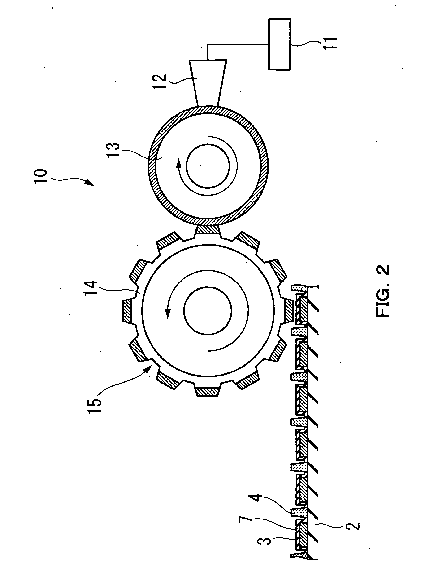
[0085] At first, as example 1, organic luminous layer 8 was formed by relief printing. Organic electroluminescent device was produced.

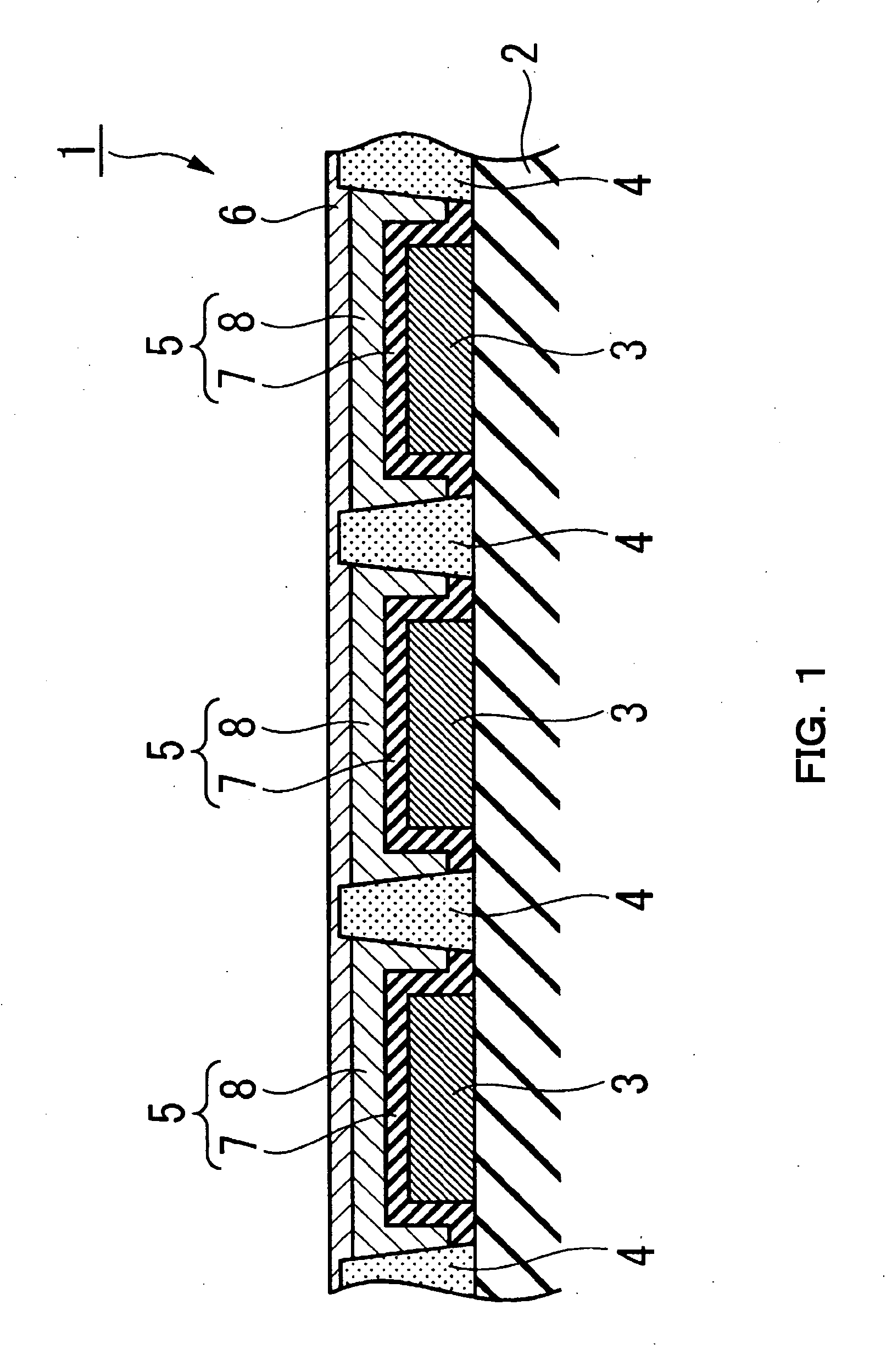
[0086] Translucency substrate 2 is explained below. It was glass of 100 mm square, and its thickness was 0.7 mm.

[0087] Transparent electrode layer 3 of configuration of a long strip of paper was formed. Width of transparent electrode layer 3 was 80 μm, and the thickness was 0.15 μm. Pitch of transparent electrode layer 3 was 120 μm.

[0088] The surface roughness Ra of transparent electrode layer 3 was 20 nm in every domain of 200 μm2.

[0089] In addition, the profile of partition wall 4 was trapezoid. The length of a side of a bottom part of trapezoid was 30 μm. The length of a side of the top of trapezoid was 15 μm. The height of trapezoid was 1 μm.

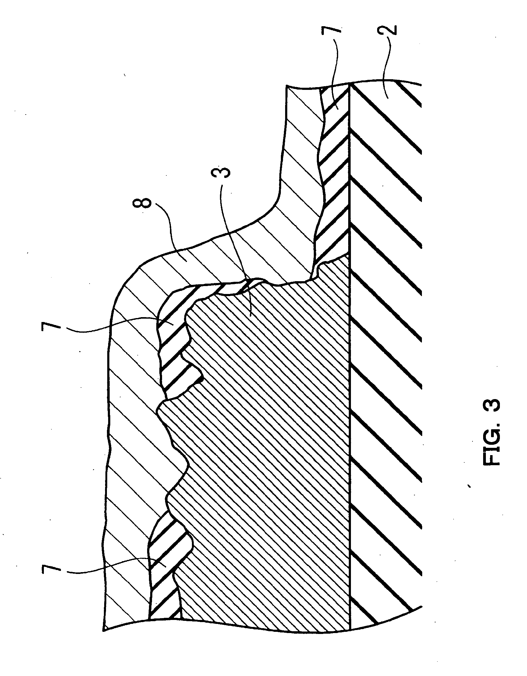
[0090] A formation method of partition wall 4 is described below. By using a photosensitive r...

Example

EXAMPLE 2

[0101] Organic electroluminescent device was produced by means of forming organic luminous layer 8 by inversion offset printing next. About organic luminous layers 8, every printing of each color, they were dried under inert atmosphere at 160 degrees Celsius for 30 minutes. The thickness was 70 nm.

[0102] Voltage was applied to transparent electrode layer 3 and counter electrode layer 6 of organic electroluminescent device 1 produced in this way. The display test result that luminance was 8500 cd / cm2 in 10V applied voltage was provided. The luminescence failure pixel was not recognized.

Example

EXAMPLE 3

[0103] Organic electroluminescent device was produced by means of forming organic luminous layer 8 by ink jet process next. In addition, illustration of a point same as example 1 is omitted in the embodiment.

[0104] About organic luminous layers 8, every printing of each color, they were dried under inert atmosphere at 150 degrees Celsius for 30 minutes. The thickness was 70 nm.

[0105] Voltage was applied to transparent electrode layer 3 and counter electrode layer 6 of organic electroluminescent device 1 produced in this way. The display test result that luminance was 8700 cd / cm2 in 10V applied voltage was provided. The luminescence failure pixel was not recognized.

[0106] In addition, the present invention is not limited by the above described embodiment. As for the present invention, various kinds of modification is possible in the range which does not deviate from general meaning of the present invention. By way of example only, in the above described embodiment, even ...


PUM

PropertyMeasurementUnit
Massaaaaaaaaaa
Molecular weightaaaaaaaaaa
Areaaaaaaaaaaa

Abstract

The present invention provides a manufacturing method of organic electroluminescent device and the organic electroluminescent device that unevenness in the surface of the transparent electrode layer is covered by the organic luminescence media layer without being affected by the unevenness.
In a manufacturing method of the organic electroluminescent device which emits light by applying voltage to organic luminous layer 5 between transparent electrode layer 3 and a counter electrode layer 6, organic luminous layer 8 is formed by using ink containing low molecular organic luminescent material of which molecular weight is less than or equal to 5000.

Description

CROSS REFERENCE [0001] This application claims priority to Japanese application number 2005-193537, filed on Jul. 1, 2005, which is incorporated by reference. BACKGROUND OF THE INVENTION [0002] 1. Field of the Invention [0003] The present invention is related to a manufacturing method of an organic electroluminescent device using electroluminescent phenomena of organic thin film and an organic electroluminescent device. [0004] 2. Description of the Related Art [0005] Organic electroluminescent device is explained below. [0006] Organic electroluminescent device includes organic a luminous layer of electroconductivity and a transparent electrode layer and a counter electrode layer which are placed on either side of this organic luminous layer. As for the organic electroluminescent device, transparent electrode layer, organic luminous layer and counter electrode layer are laminated on a substrate of translucency by this sequence. [0007] And, by means of applying voltage to organic lumi...

Claims


Application Information

Patent Timeline
IPC IPC(8): H01L51/54H01L51/56
CPCH01L27/3211H01L51/0004H01L27/3283H01L27/3246H10K59/35H10K59/122H10K59/173H10K71/13
Inventor TAGUCHI, TAKAOKITAZUME, EIICHIUCHIBORI, AKIKO
Owner TOPPAN PRINTING CO LTD
Why Eureka
Try Eureka