Area efficient memory architecture with decoder self test and debug capability

Active Publication Date: 2007-01-04
STMICROELECTRONICS PVT LTD
View PDF22 Cites 11 Cited by
  • Summary
  • Abstract
  • Description
  • Claims
  • Application Information

AI Technical Summary

Benefits of technology

[0015] One embodiment of the invention is a test architecture / methodology for an address decoder that reduces the test time and at the same time provides the ability to reliably detect and segregate the address decoder faults from other types of faults. One embodiment of the present invention solves all the problems created by the mentioned disadvantages in the memory address decoder fault testing using the prior art test schemes. Additionally, one embodiment of the present invention results in high-speed memories with negligible area overhead.
[0018] One embodiment of the invention provides a memory architecture resulting in lower access time.
[0019] One embodiment of the instant invention provides reliable test results for memory address decoder.
[0051] One embodiment of the present invention provides an area efficient memory and an integrated method for decoder self-test and debug capability. The modified memory address decoder has additional blocks within the new memory architecture for the self-test and debug operation. While the memory results in some additional area overhead when compared to the external BIST testing of the decoder, the added blocks are full custom and hence are very area efficient. Additionally, the memory gives a better access and cycle time and has negligible impact on address setup and hold time requirements. The power consumption is nearly the same as well.

Problems solved by technology

The miniaturization of devices has also resulted in increased complexity and consequently higher clock speeds for integrated circuits.
As ASIC designs become more memory dominated, the probability of memory errors has increased due to manufacturing faults and process variations.
These BISTs perform failure testing on the memories at very high clock speeds.
This is a major bottleneck for the development of reliable high-speed ASICs as most of the current BIST architectures do not provide reliable memory testing at high clock speeds.
The few current BIST devices that do provide reliable testing are very inefficient in terms of operation speed.
Manufacturing defects in the address decoder can result in faults like stuck-at on the word lines, wrong selection and multiple word line selections.
These faults arise when the setup or hold time requirements for decoder latches are not met or there are some other timing problems with the block.
The limitation of the aforementioned patent document is that it does not suggest high speed and minimal clock cycle testing of the memory address decoder.
These algorithms have several disadvantages as they are highly unreliable in detecting the address decoder faults.
Hence, the test time for memory address decoder is very large if the memory size is big.
Some other kinds of faults like coupling faults or IO faults may mask the address decoder faults as the fault is detected through the memory output port.
There is no way of viewing the address decoder faults as the paths come out through the memory core.
Debugging the address decoder faults is very hard as segregating the decoder faults from other faults is not possible.

Method used


Image

  • Area efficient memory architecture with decoder self test and debug capability
  • Area efficient memory architecture with decoder self test and debug capability
  • Area efficient memory architecture with decoder self test and debug capability

Examples


Embodiment Construction

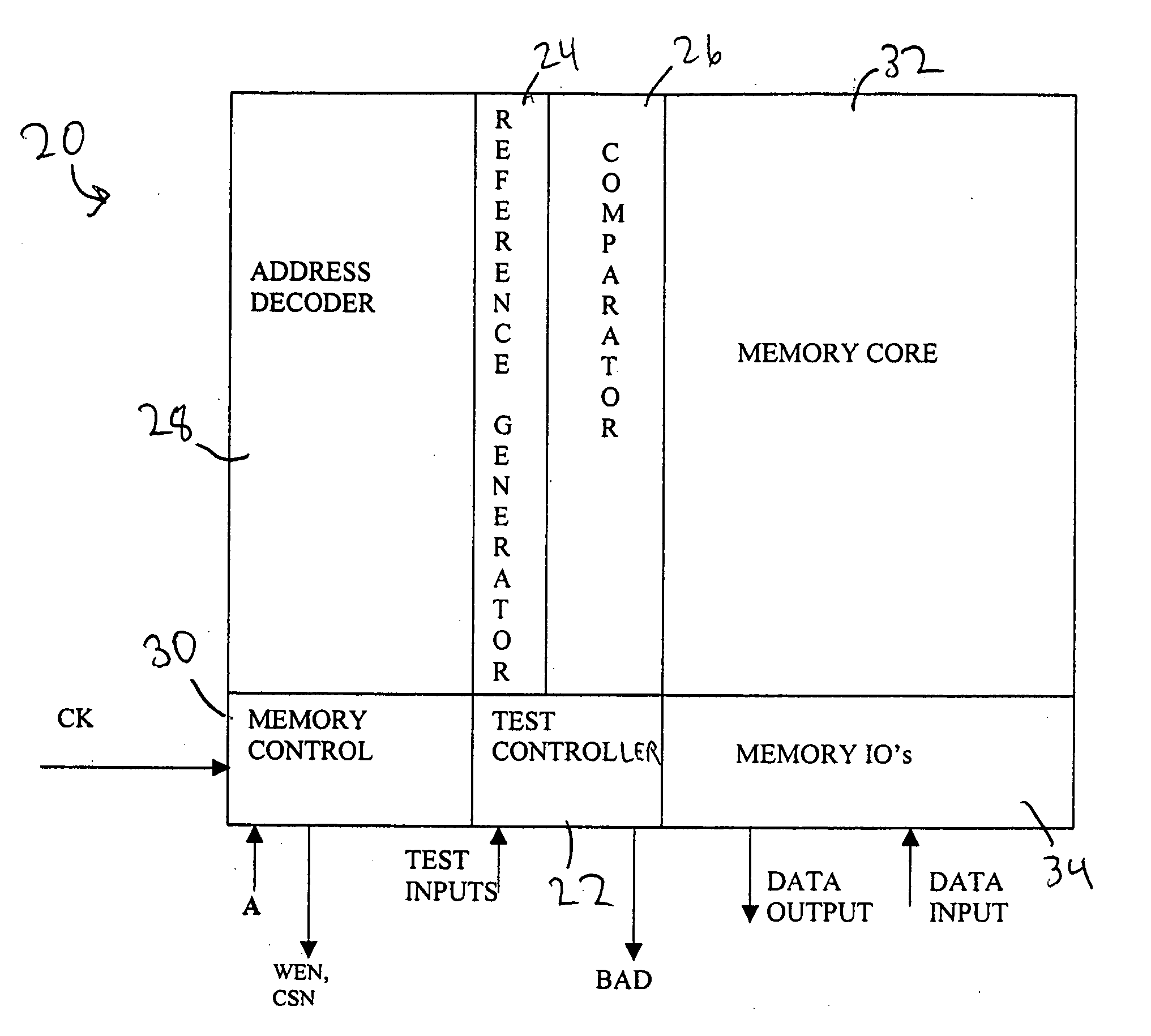
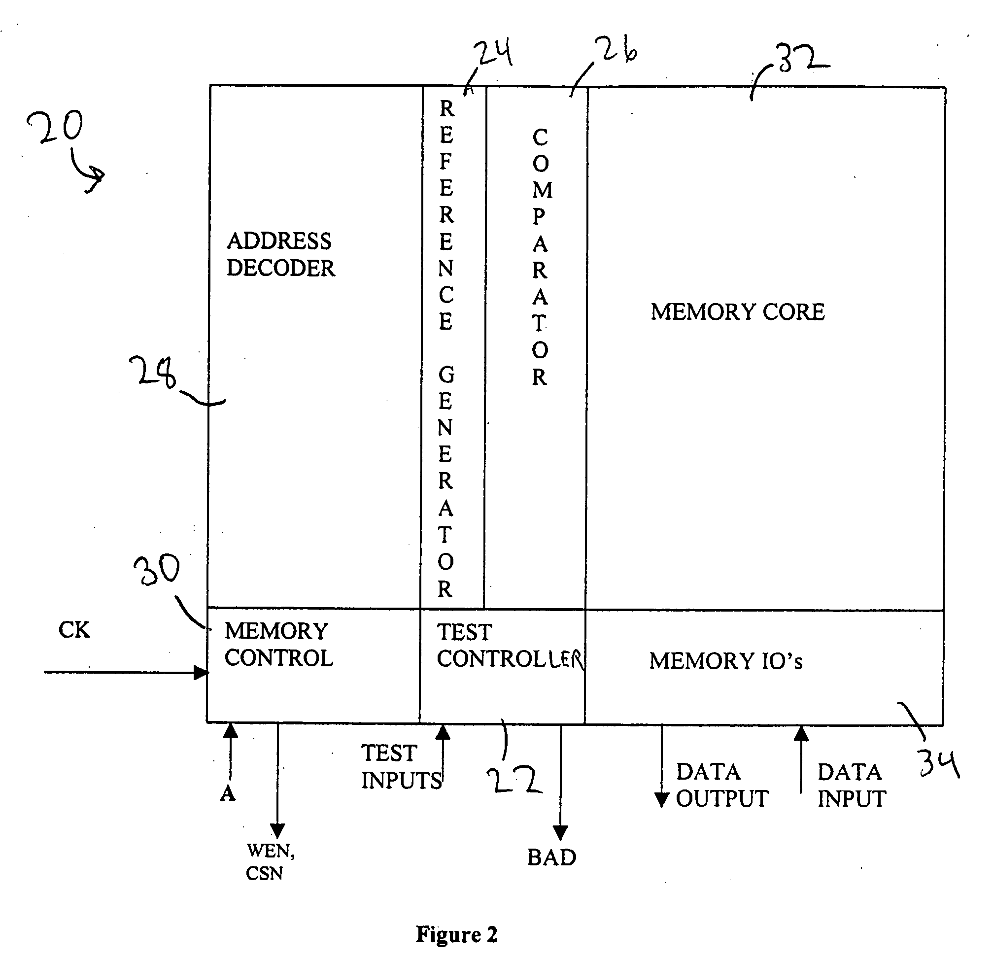
[0060] One embodiment of the current invention is a complete memory address decoder test solution for a high-speed memory from design to test. The test solution has been designed to keep the performance aspect in mind and has resulted in area and speed efficient memory architecture. Further the memory with integrated decoder test device is designed to operate in test mode, debug mode and memory operation mode for complete testing and debugging of the memory address decoder. The integrated test device is also used as a pipelining device in normal memory operation mode to reduce the memory access time.

[0061] The block diagram of a single port memory device 20 according to one embodiment of the invention is illustrated in FIG. 2. However, the invention is not limited to a single port memory and a similar architecture can be implemented for any memory by introducing a separate test device for each individual decoder. The memory device 20 includes a test controller 22, a reference gener...


PUM


Abstract

An integrated test device reduces external wiring congestion to a memory. The integrated test device provides for separate decoder testing and debugging to find specific errors in the memory. The device also helps in reducing the complexity of the test of external BIST. Furthermore, the number of clock cycles required for the decoder testing for an N-address memory is reduced from 4N cycles to N clock cycles. Additionally, the access time for the memory is reduced as the test device is used as a pipelining device in normal operation mode.

Description

BACKGROUND OF THE INVENTION [0001] 1. Field of the Invention [0002] The present invention relates to improved area efficient memory architecture with decoder self test and debug capability. More particularly, it relates to providing an integrated test architecture / methodology within the memory for high-speed address decoder testing and high speed memory operation. [0003] 2. Description of the Related Art [0004] Over the years, semiconductor devices have become considerably smaller and faster. The semiconductor technology trends have consistently followed Moore's Law as the technology has shrunk by a factor of 1.5 every year. The miniaturization of devices has also resulted in increased complexity and consequently higher clock speeds for integrated circuits. For instance, complex application specific integrated circuits (ASICs) today have several million transistors on a single chip. Since these chips can hold more transistors, a single chip has more logic blocks. As a result, on-chi...

Claims


Application Information

Patent Timeline
IPC IPC(8): G11C29/00
CPCG11C2029/1206G11C29/02G11C29/024G11C5/025
Inventor DUBEY, PRASHANT
Owner STMICROELECTRONICS PVT LTD
Why Eureka
Try Eureka