Electron emitting composite based on regulated nano-structures and a cold electron source using the composite

a composite and electron source technology, applied in the field of controlled electron emission of cold electron sources, can solve the problems of low yield, high cost and low yield associated with the fabrication process, and the hope of deriving an electron source of high emission site density from a vertically aligned cnt array has largely unfulfilled, and achieves low modulation voltage, high emission site and current density, and high aspect ratio

Inactive Publication Date: 2007-01-04
TOLT ZHIDAN L
View PDF9 Cites 42 Cited by
  • Summary
  • Abstract
  • Description
  • Claims
  • Application Information

AI Technical Summary

Benefits of technology

[0043] One advantage of the present invention is that an integrated gate electrode can be conveniently built on top of the fragile nano-structures.
[0044] Another advantage is that a lower modulation voltage is derived from the integrated gate structure and additional field enhancement at the emitting tip from the formation of triple junctions and higher aspect ratio.
[0045] Yet another advantage is that a higher emission site and current density are derived from the higher density of nano-structures embedded in a matrix with substantially equalized tip to gate distance and tip apex.
[0046] Other advantages include: (a) a higher degree of collimation of the electron beam derived from regulated emission direction from each emitter; (b) longer lifetime and consistent emission performance derived from a consistent local electrical field at each emitting tip as the tip erodes from ion bombardment, mechanical protection, thermal and electrical conduction enhancement from the embedding matrix, and lower ion sputter yields of the selected nano-structure and embedding materials; and (c) a higher production yield and an increase in ease of fabrication derived from embedding the nano-structure in an insulating matrix and protection of the nano-structure from the matrix.

Problems solved by technology

The high cost and low yield associated with its fabrication process, and the high susceptibility of the tip to contamination and ion bombardment have effectively prevented this technology from wide application.
As a result, the hope of deriving an electron source of high emission site density from a vertically aligned CNT array has largely unfulfilled.
Two major problems plague these random CNT films.
First, emission is inhomogeneous and often dominated by strong sites so that the emission site density is still relatively low despite of improvement over vertically aligned CNTs.
Second, it is difficult to fabricate a gate electrode on top of these films without degrading their emission properties.
Such a large distance results in high driving voltage, and the emission from underneath the grid goes directly to the grid without contributing to the output current.
The difficulty in accurately and uniformly mounting and maintaining a fine grid over large area with a small gap is another hurdle.
However, the emission performance from these films is worse than when the film is directly grown on the surface.
Such variation, plus the electrostatic screening effect between CNTs in the same gate hole, causes an emission dominated by the ones closer to the gate in each gate hole, and changes the emission threshold field from gate hole to gate hole, resulting in a source of little practical use.
The device still does not address the problem of a varying CNT in its height and aspect ratio in each gate hole and there is little emitter redundancy built in.
Also, due to the large inter-tube spacing, CNT grow thick, reducing the aspect ratio and therefore increasing the driving voltage.

Method used


Image

  • Electron emitting composite based on regulated nano-structures and a cold electron source using the composite
  • Electron emitting composite based on regulated nano-structures and a cold electron source using the composite
  • Electron emitting composite based on regulated nano-structures and a cold electron source using the composite

Examples


Embodiment Construction

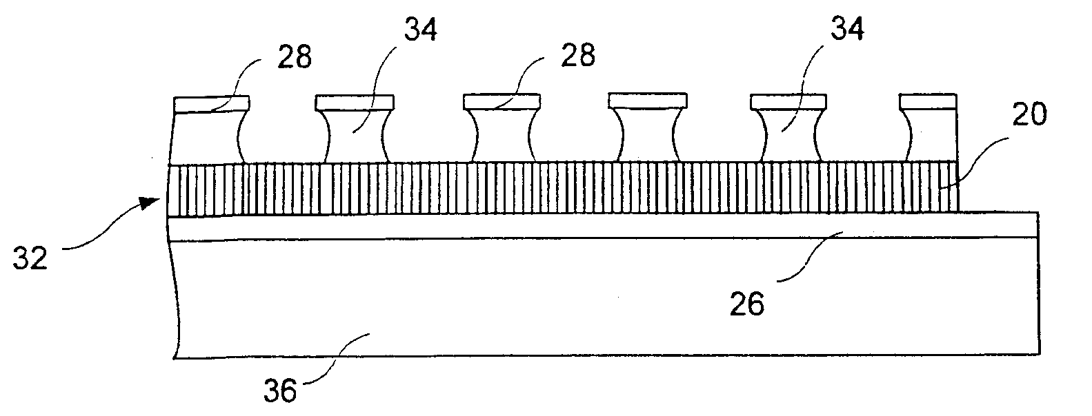
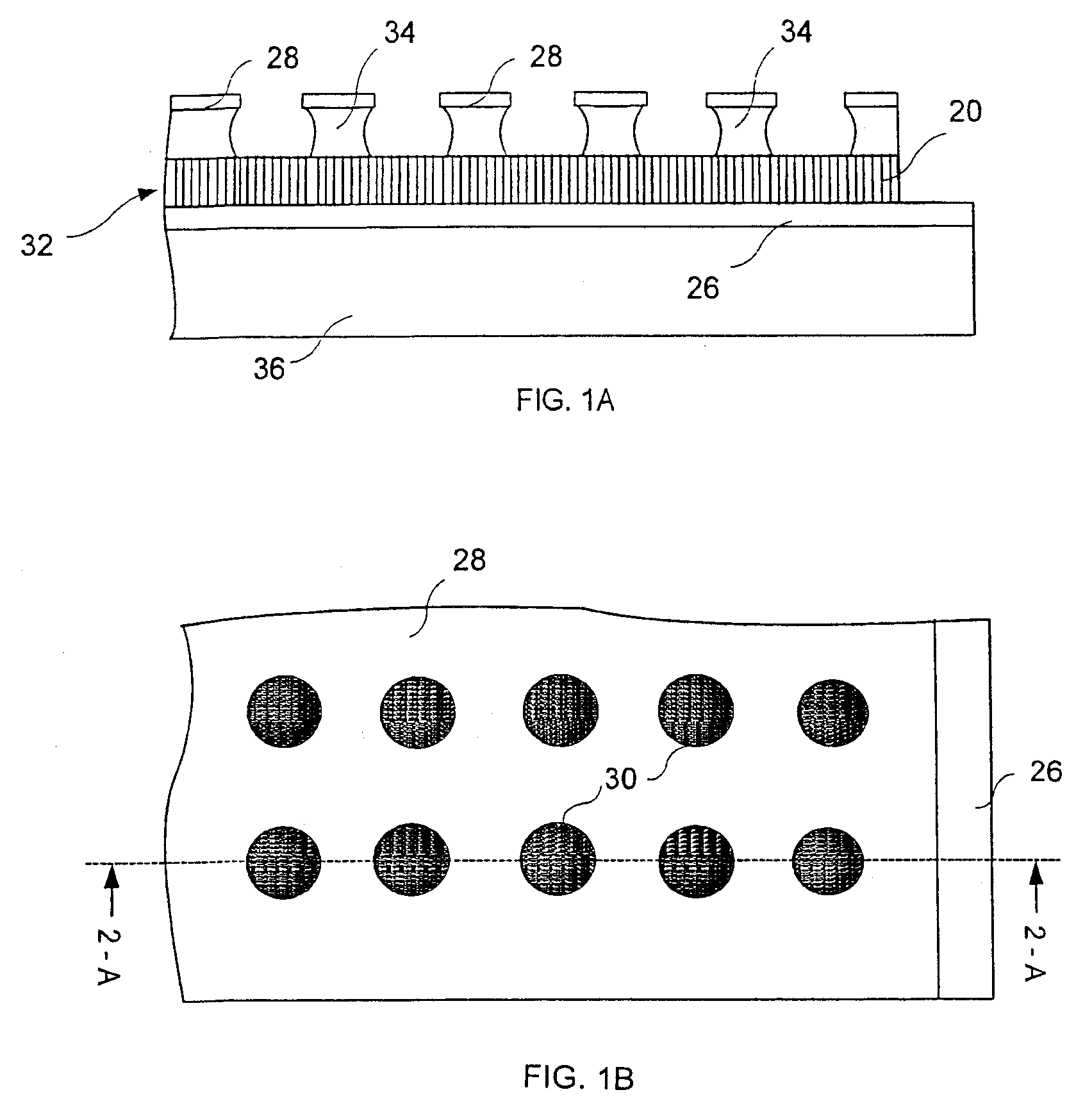
[0086]FIG. 1 illustrates an electron source by current invention using vertically aligned CNT 20. It includes a substrate 36, a cathode 26 deposited on the substrate, an emitter layer 32, a gate electrode 28 insulated from the emitter layer by a gate insulator 34. Apertures 30 are opened in the gate electrode and gate insulator to extract electrons from the exposed CNT tips in the emitter layer 32.

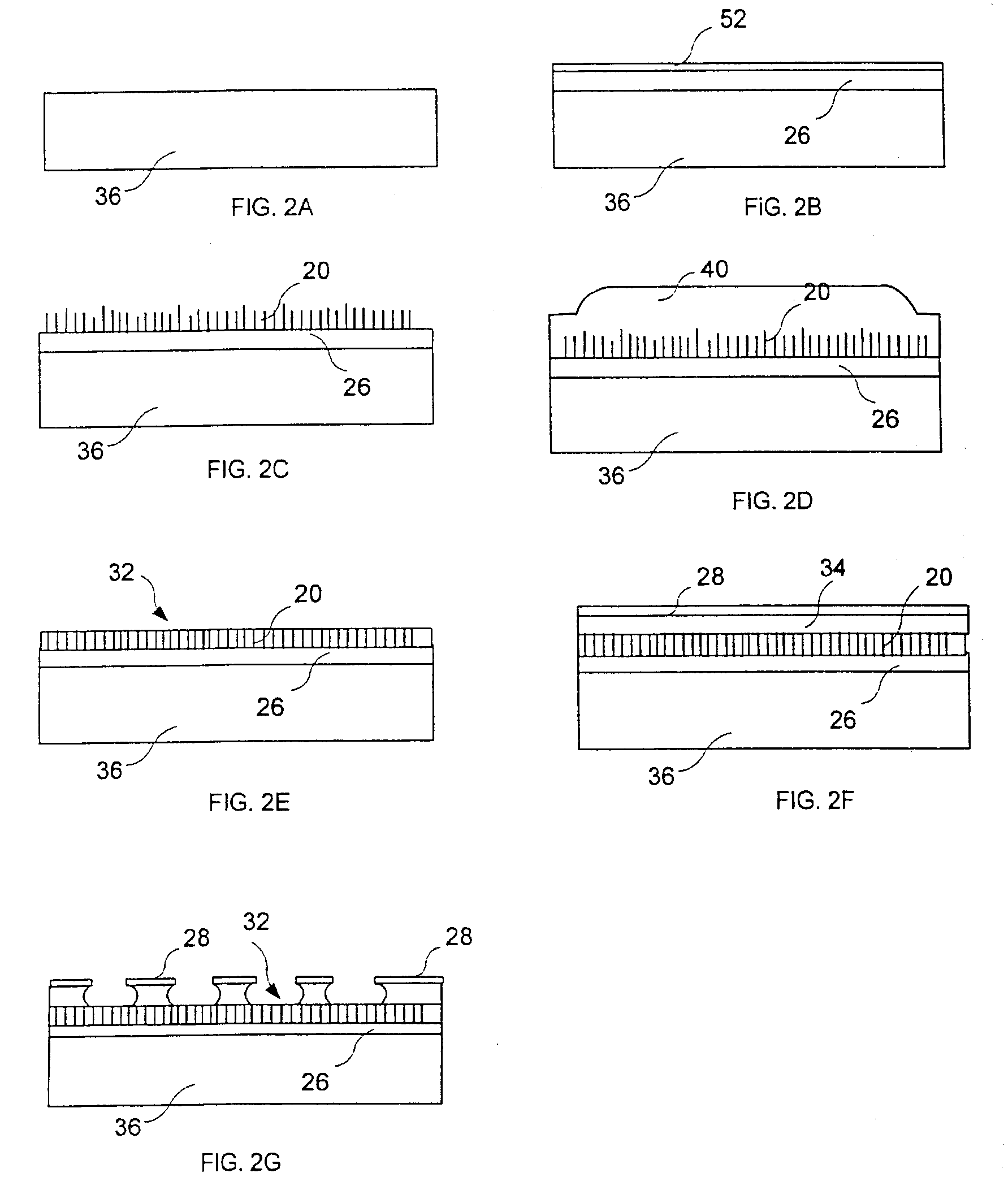
[0087]FIG. 2 depicts one of possible fabrication process flows for the source shown in FIG. 1. The process starts with a substrate 36 shown in FIG. 2A. Examples are Si or glass. A first conductive cathode layer 26 and a thin catalyst layer 52 are then deposited, as is shown in FIG. 2B. Examples of the first conductive layer and catalyst are Cr and Ni respectively. The conductive layer should be chosen so that it does not prohibit CNT growth with the presence of catalyst. The catalyst layer is made of many Ni dots of nanometer size. An array of vertically aligned CNT 20 is then grown, as s...


PUM

PropertyMeasurementUnit
lengthaaaaaaaaaa
thicknessaaaaaaaaaa
thicknessaaaaaaaaaa

Abstract

A field emission electron source includes a substrate, a first conductive electrode terminated to provide electrons, an emitting composite layer for emitting electrons, and a second electrode insulated from the emitter layer and terminated to extract electrons through vacuum space. The emitting composite layer lies between and parallel to the said first and the second electrodes, and comprises nano-structures embedded in a solid matrix. One end of the nano-structures is truncated and exposed at the surface of the emitter layer so that both the length and the apex of the nano-structure are regulated and the exposed nano-tips are kept substantially the same distance from the gate electrode. The embedding material is chosen to form triple junctions with the exposed tip to further enhance the field.

Description

CROSS REFERENCE TO RELATED APPLICATIONS [0001] This application claims priority to and incorporates by reference each of the following applications: [0002] U.S. Provisional Application titled ELECTRON SOURCE BASED ON REGULATED NANO-STRUCTURED MATERIALS, Ser. No. 60 / 457,210, filed Mar. 24, 2003; [0003] U.S. Provisional Application titled COLD ELECTRON SOURCE BASED ON REGULATED NANO-STRUCTURED MATERIALS, Ser. No. 60 / 491,570, filed Jul. 30, 2003; and [0004] U.S. Provisional Application titled ELECTRON EMITTING COMPOSITE BASED ON REGULATED NANO-STRUCTURES AND A COLD ELECTRON SOURCE USING THE COMPOSITE, Ser. No. 60 / 521,135, filed Feb. 24, 2004. [0005] This application also claims the benefit of U.S. patent application Ser. No. 10 / 807,890, titled “ELECTRON EMITTING COMPOSITE BASED ON REGULATED NANO-STRUCTURES AND A COLD ELECTRON SOURCE USING THE COMPOSITE,” filed Mar. 24, 2004.BACKGROUND OF INVENTION [0006] The present invention relates generally to the emission of electrons from nano-str...

Claims


Application Information

Patent Timeline
Patent Type & Authority Applications(United States)
IPC IPC(8): H01J9/04D01F9/12
CPCB82Y10/00H01J1/304H01J2201/30469H01J9/025H01J3/022
Inventor TOLT, ZHIDAN L.
Owner TOLT ZHIDAN L
Why Eureka
Try Eureka