Method of manufacturing flash memory device

a technology of flash memory and manufacturing method, which is applied in the direction of semiconductor devices, basic electric elements, electrical apparatus, etc., can solve the problems of low reliability of devices, difficult application of methods, breakdown voltage, etc., and achieve the effect of reducing interference phenomena and improving capacitan

Inactive Publication Date: 2007-01-04
SK HYNIX INC
View PDF13 Cites 29 Cited by
  • Summary
  • Abstract
  • Description
  • Claims
  • Application Information

AI Technical Summary

Benefits of technology

[0006] In one embodiment, the invention provides a method of manufacturing a flash memory device, which can improve capacitance and reduce the interference phenomenon.

Problems solved by technology

If the high dielectric material is used as the dielectric layer, however, the interface trap characteristic is degraded and the threshold voltage is abruptly shifted, resulting in low reliability of the devices.
Accordingly, it is difficult to apply the method.
Furthermore, if the thickness of the dielectric layer is reduced, the breakdown voltage is lowered, which has a direct effect on data failure.
As a result, it is difficult to secure the characteristics and uniformity of the devices.

Method used


Image

  • Method of manufacturing flash memory device
  • Method of manufacturing flash memory device
  • Method of manufacturing flash memory device

Examples


first embodiment

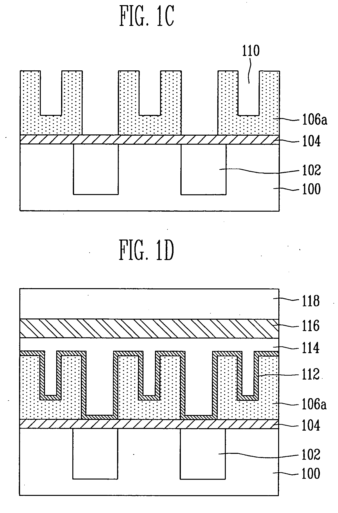
[0024]FIGS. 1A to 1D are cross-sectional views illustrating a method of manufacturing a flash memory device according to the invention.

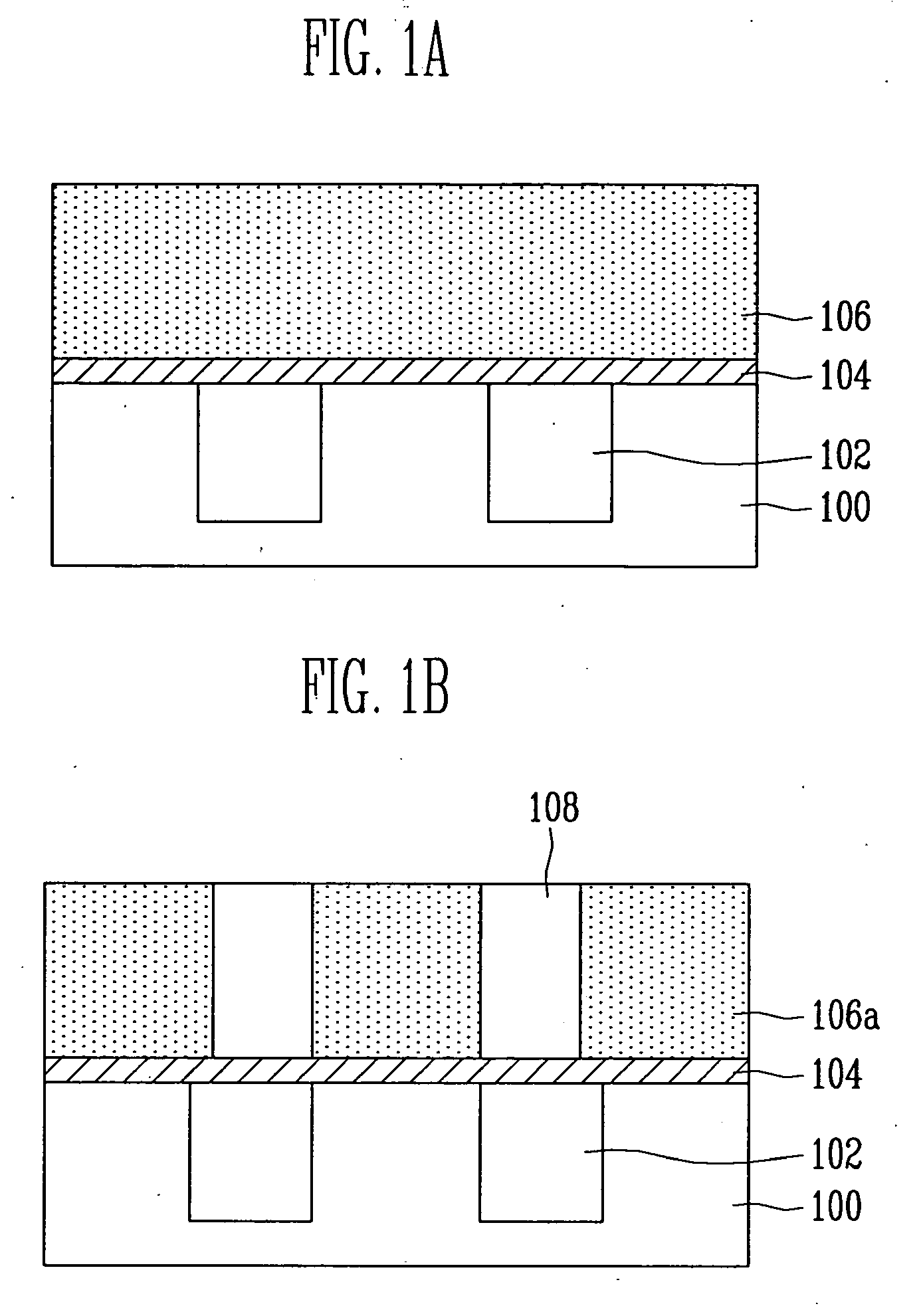
[0025] Referring to FIG. 1A, a tunnel oxide layer 104 and a conductive layer 106 for a floating gate are sequentially deposited on a semiconductor substrate 100 in which isolation structures 102 are formed. The conductive layer 106 may be preferably formed using any one of a polysilicon layer, W, WN, Ti, TiN, Pt, Ru, RuO2, Ir, IrO2, and Al, or combination thereof by means of a CVD method or an ALD method. More particularly, the doped polysilicon layer may be preferably formed to a thickness of 100 Å to 5000 Å at a temperature of 250° C. to 1000° C.

[0026] Referring to FIG. 1B, a first photoresist pattern (not shown) is formed on the conductive layer 106 over the isolation structures 102. The conductive layer 106 is etched using the first photoresist pattern as a mask, thus forming conductive layer patterns 106a. The first photoresist pattern is strip...

second embodiment

[0035]FIGS. 2A to 2F are cross-sectional views illustrating a method of manufacturing a flash memory device according to the invention.

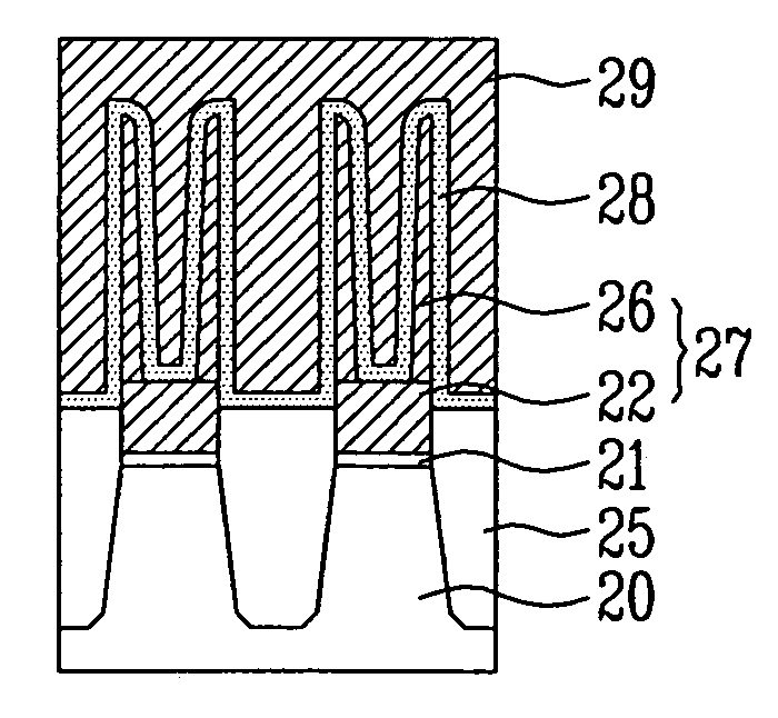
[0036] Referring to FIG. 2A, a tunnel oxide layer 21, a first conductive layer 22 for a floating gate, and a hard mask layer 23 are sequentially formed on a semiconductor substrate 20. The hard mask layer 23, the first conductive layer 22, the tunnel oxide layer 21, and a predetermined depth of the semiconductor substrate 20 are etched to form a trench 24. A lateral oxidization process is performed in order to remove damage that has occurred during the etch process of the trench 24. The first conductive layer 22 may be formed using a polysilicon layer and the hard mask layer 23 may be formed using a nitride layer.

[0037] To facilitate the etch process of the trench, a hard mask layer may be further formed on the hard mask layer 23. The hard mask layer may be patterned and a trench etch process using the patterned hard mask layer as a mask may be then...


PUM


Abstract

A method of manufacturing a flash memory device which can improve capacitance and can reduce the interference phenomenon. According to one embodiment, a method of manufacturing a flash memory device includes the steps of depositing a tunnel oxide layer over a semiconductor substrate having a isolation structure, depositing a conductive layers for a floating gate over the tunnel oxide layer, forming an oxide layer between the conductive layers for the floating gate, forming a recess pattern in the conductive layers for the floating gate, and depositing a dielectric layer and a conductive layer for a control gate, respectively.

Description

BACKGROUND [0001] The invention relates generally to a method of manufacturing a flash memory device and more particularly, to a method of manufacturing a flash memory device, wherein capacitance can be interposed and the interference phenomenon can be reduced. [0002] In general, a flash memory device is a device that stores and reads data on the basis of variation in the threshold voltage when electrons are injected into a floating gate and when electrons are not injected into the floating gate. As the degree of integration of devices is increased, rapid operating speed and high data reliability of the flash memory device are required. To this end, it is necessary to increase the capacitance. [0003] To increase the capacitance of the flash memory device, there have been proposed a method of using a high dielectric material as the dielectric layer formed between the floating gate and the control gate, a method of reducing the thickness of the dielectric layer, a method of increasing...

Claims


Application Information

Patent Timeline
Patent Type & Authority Applications(United States)
IPC IPC(8): H01L21/336
CPCH01L21/28114H01L29/42376H01L27/11521H01L27/115H10B69/00H10B41/30
Inventor KIM, NAM KYEONGCHOI, EUN SEOKOH, SANG HYUN
Owner SK HYNIX INC
Why Eureka
Try Eureka