Process for electroless copper deposition

a technology of electroless copper and deposition process, which is applied in the direction of liquid/solution decomposition chemical coating, metallic material coating process, coating, etc., can solve the problems of poor nucleation, high aspect ratio of nanometer features, and high effort directed at the formation of substantially voids

Active Publication Date: 2007-01-04
APPLIED MATERIALS INC
View PDF10 Cites 35 Cited by
  • Summary
  • Abstract
  • Description
  • Claims
  • Application Information

AI Technical Summary

Problems solved by technology

However, as the fringes of circuit technology are pressed, the shrinking dimensions of interconnects in VLSI and ULSI technology have placed additional demands on the processing capabilities.
Many traditional deposition processes have difficulty filling nanometer-sized structures where the aspect ratio exceeds 4:1, and particularly where the aspect ratio exceeds 10:1.
Therefore, there is much effort directed at the formation of substantially void-free, nanometer-sized features having high aspect ratios.
Native oxides that are easily formed on the barrier layer may cause the poor nucleation.
However, if there are discontinuities in the seed layer across the surface, then a subsequently deposited copper-containing layer may not form uniformly to cover the seed layer.

Method used


Image

  • Process for electroless copper deposition
  • Process for electroless copper deposition
  • Process for electroless copper deposition

Examples


Embodiment Construction

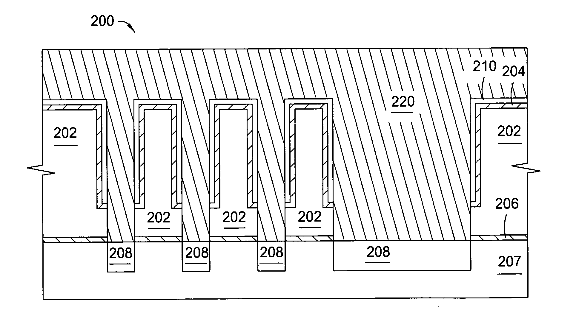
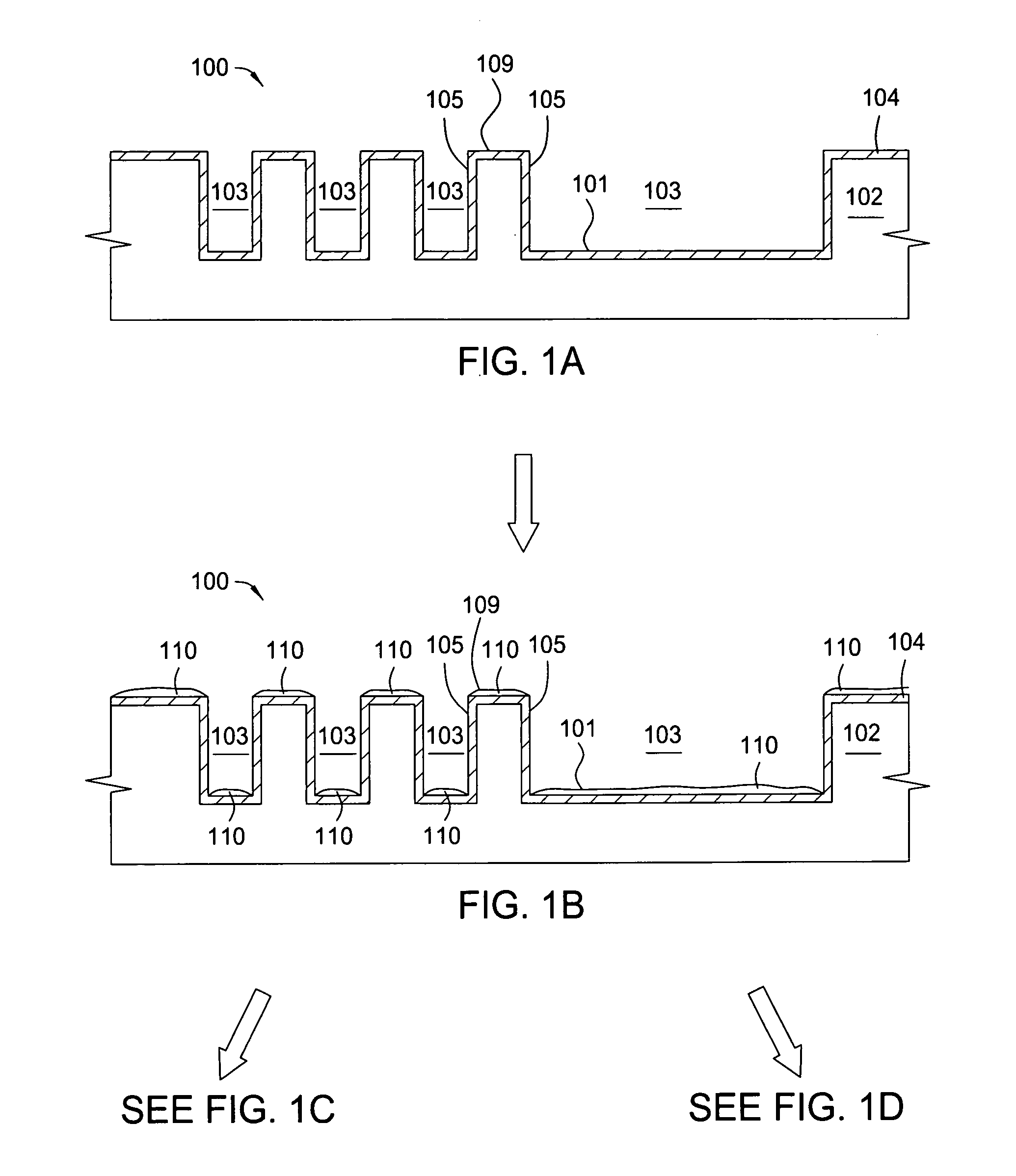
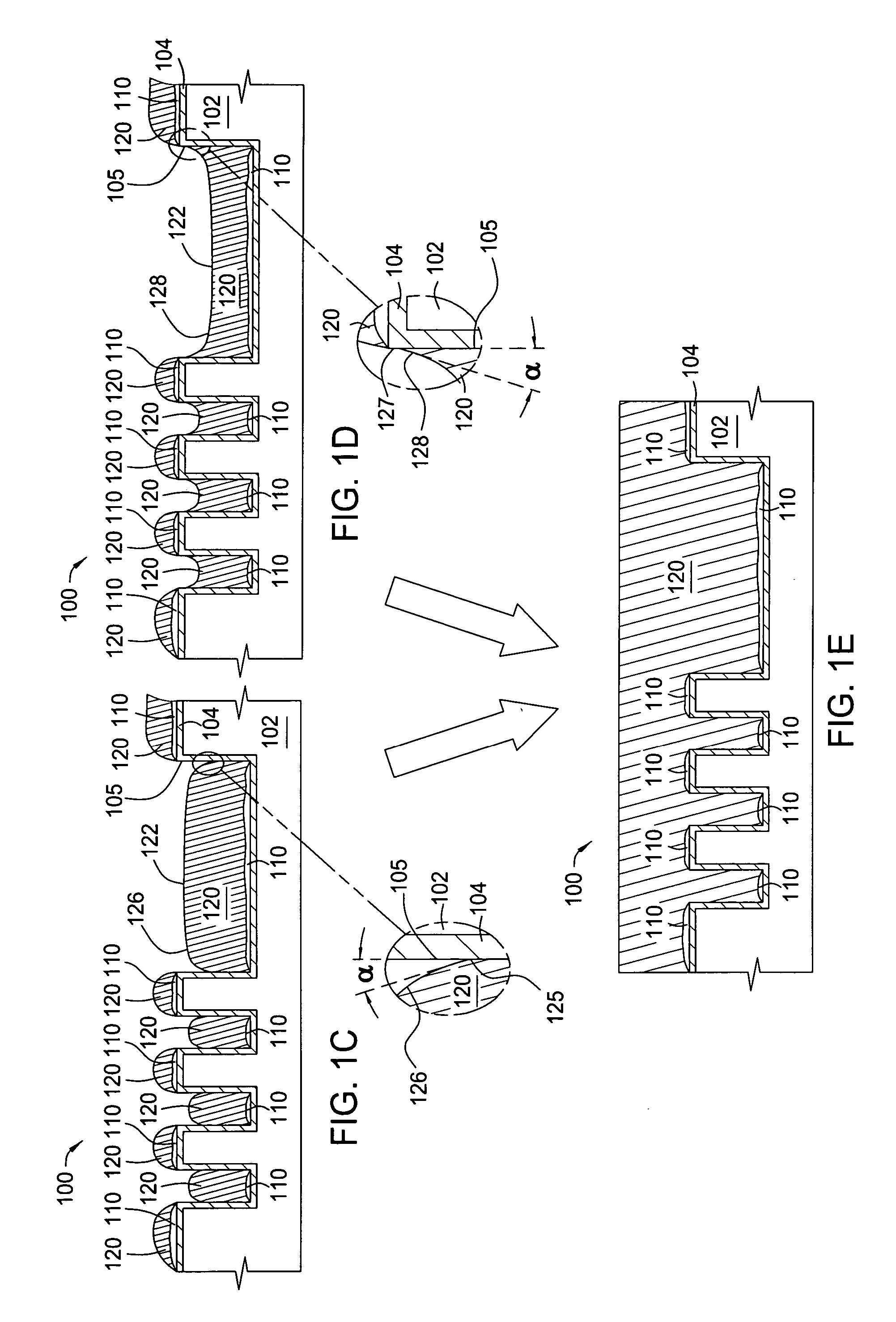
[0024] Embodiments of the invention provide methods for forming conductive materials within an aperture of a feature on a substrate surface. In one example, the method provides depositing a seed layer within the feature by a vapor deposition process. The seed layer may contain copper, ruthenium, cobalt, tantalum, titanium, tungsten, rhenium, palladium, platinum, nickel, alloys thereof, or combinations thereof. Once the seed layer has been deposited, the feature may be bottom up filled with a copper-containing material during an electroless deposition process. The electroless deposition process may employ an innovative copper deposition solution to ensure that features are free of defects, such as voids or seams. The seed layer may be deposited directly onto a contact surface or on a barrier layer.

[0025] In one embodiment, the seed layer is selectively deposited by a collimated physical vapor deposition (PVD) process on the bottom surface of the feature while maintaining the sidewal...


PUM

PropertyMeasurementUnit
angleaaaaaaaaaa
angleaaaaaaaaaa
angleaaaaaaaaaa

Abstract

Embodiments of the invention provide methods for forming conductive materials within contact features on a substrate by depositing a seed layer within a feature and subsequently filling the feature with a copper-containing material during an electroless deposition process. In one example, a copper electroless deposition solution contains levelers to form convexed or concaved copper surfaces. In another example, a seed layer is selectively deposited on the bottom surface of the aperture while leaving the sidewalls substantially free of the seed material during a collimated PVD process. In another example, the seed layer is conformably deposited by a PVD process and subsequently, a portion of the seed layer and the underlayer are plasma etched to expose an underlying contact surface. In another example, a ruthenium seed layer is formed on an exposed contact surface by an ALD process utilizing the chemical precursor ruthenium tetroxide.

Description

CROSS-REFERENCE TO RELATED APPLICATIONS [0001] This application claims benefit of U.S. Ser. No. 60 / 663,492, (APPM / 009920L), entitled “Electroless Copper Deposition,” filed Mar. 18, 2005, which is herein incorporated by reference in its entirety.BACKGROUND OF THE INVENTION [0002] 1. Field of the Invention [0003] Embodiments of the invention generally relate to methods for depositing materials within a feature, and more specifically to methods for depositing a seed layer prior to filling a contact plug with a copper-containing material by an electroless deposition process. [0004] 2. Description of the Related Art [0005] Reliably producing nanometer-sized features is one of the key technologies for the next generation of very large scale integration (VLSI) and ultra large scale integration (ULSI) of semiconductor devices. However, as the fringes of circuit technology are pressed, the shrinking dimensions of interconnects in VLSI and ULSI technology have placed additional demands on the...

Claims


Application Information

Patent Timeline
Patent Type & Authority Applications(United States)
IPC IPC(8): H01L21/44
CPCC23C18/38H01L21/288H01L21/76844C23C18/1831H01L21/76874C23C18/1608C23C18/165H01L21/76846
Inventor LUBOMIRSKY, DMITRYWEIDMAN, TIMOTHY W.SHANMUGASUNDRAM, ARULKUMARKOVARSKY, NICOLAY Y.WIJEKOON, KAPILA
Owner APPLIED MATERIALS INC
Why Eureka
Try Eureka