

Non-volatile semiconductor memory device
a semiconductor memory and non-volatile technology, applied in static storage, digital storage, instruments, etc., can solve the problems of deterioration of memory cell characteristics, long time-consuming verification operation, and increased voltage stress application number, and achieve high speed
- Summary
- Abstract
- Description
- Claims
- Application Information
AI Technical Summary
Benefits of technology
Problems solved by technology
Method used
Image

Examples
embodiment 1
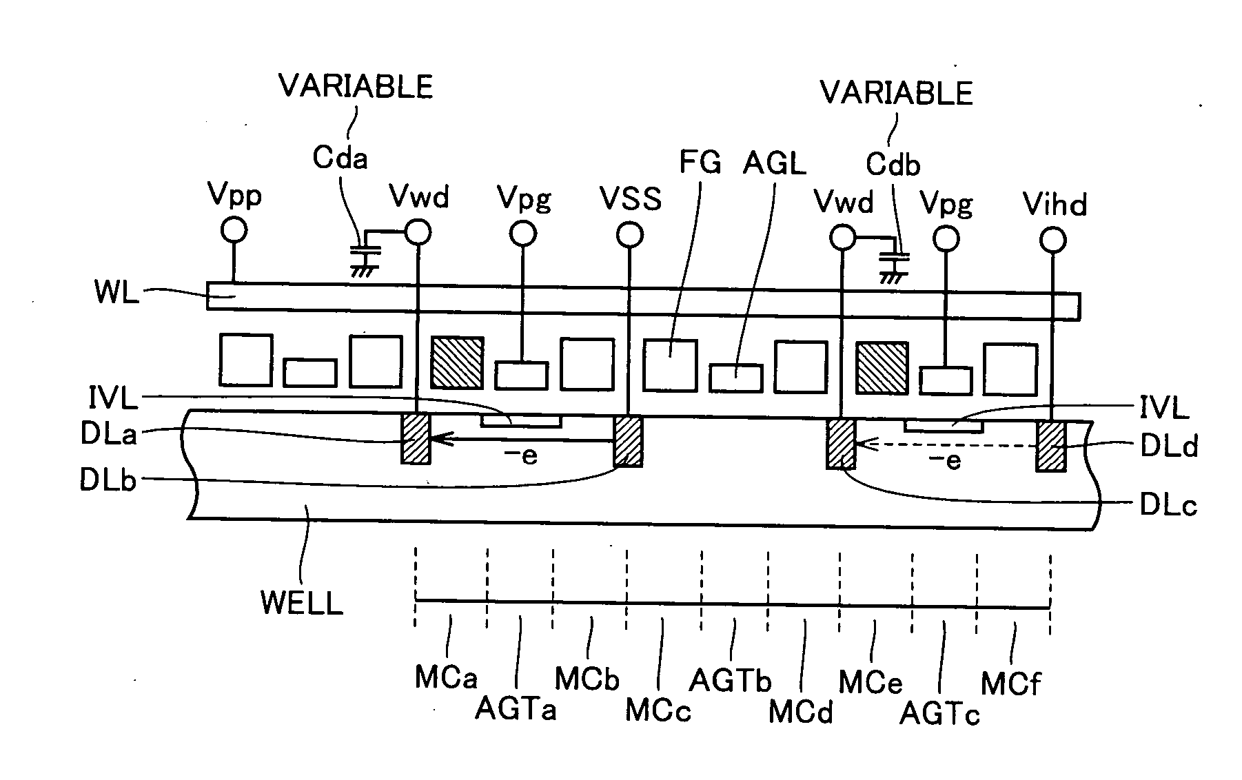
[0077]FIG. 1 schematically shows an arrangement of memory cells of a non-volatile semiconductor memory device to which the present invention is applied. Referring to FIG. 1, memory cells MCa to MCd are connected to a word line WL. Between memory cells MCa and MCb, an assist gate AGTa is arranged, and between memory cells MCc and MCd, an assist gate AGTb is arranged. To these assist gates AGTa and AGTb, assist gate selecting signals AG0 and AG1 are applied, respectively.
[0078] Memory cells MCa to MCc are formed of stacked gate type transistors having a floating gate, and a node opposite to a node connected to the assist gate is connected to a diffusion line DL (DLa to DLc) formed of an impurity diffusion layer of low resistance.
[0079] Assist gates AGTa and AGTb continuously extend in the column direction, in the same direction as diffusion lines DLa to DLc, and form inverted layers at the surface of substrate regions immediately below the gates, in accordance with assist gate selec...
embodiment 2
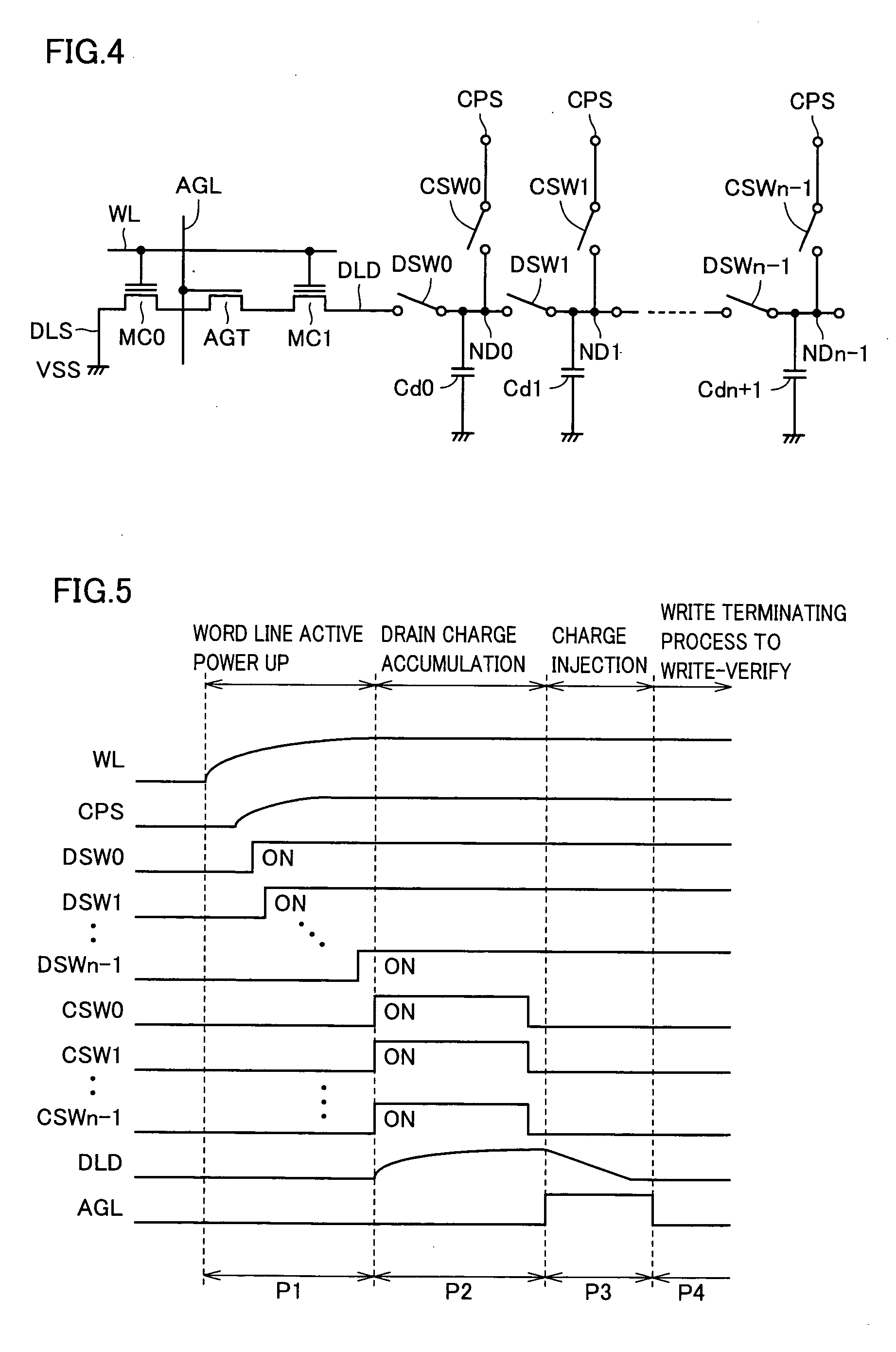
[0133]FIG. 8 schematically shows a configuration of a main portion of a non-volatile semiconductor memory device according to Embodiment 2 of the present invention. The configuration shown in FIG. 8 differs from that of FIG. 4 in the following point. Specifically, in the configuration shown in FIG. 8, capacitance element Cs is connected also to the source node DLS of memory cell MC0. Except for this point, the configuration shown in FIG. 8 is the same as that of FIG. 4. Therefore, corresponding portions are denoted by the same reference characters and detailed description thereof will not be repeated.
[0134] In Embodiment 2 of the present invention, charges are distributed between capacitance Dc (combined capacitance of capacitances used among Cd0 to Cdn−1) of drain node DLD and capacitance Cs connected to the source node (diffusion line) DLS, so that a current is caused to flow between the source / drain of the memory cell and data is written in accordance with source side injection ...
embodiment 3
[0146]FIG. 10 schematically shows an overall configuration of a non-volatile semiconductor memory device according to Embodiment 3 of the present invention. The non-volatile semiconductor memory device shown in FIG. 10 implements the configurations of Embodiments 1 and 2 described above.
[0147] Referring to FIG. 10, the non-volatile semiconductor memory device includes memory array groups MG0 to MG(M−1) each including a plurality of (in the example of FIG. 10, four) memory arrays. Memory array group MG0 includes memory arrays MA0 to MA3, and memory array group MG(M−1) includes memory arrays MA(N−4) to MA(N−1). In each of the memory arrays MA to MA(N−1), the internal configuration of which will be describe in detail later, memory cells are arranged in a matrix of rows and columns. A word line is provided corresponding to each row of memory cells, and a bit line is provided corresponding to each column of memory cells, to be shared by adjacent columns. In FIG. 10, a global bit line GB...
PUM
 Abstract
Description
Claims
Application Information