
Magnetoresistive device, thin film magnetic head, head gimbals assembly, head arm assembly, magnetic disk apparatus, synthetic antiferromagnetic magnetization pinned layer, magnetic memory cell, and current sensor

Active Publication Date: 2007-01-25
TDK CORPARATION
View PDF8 Cites 34 Cited by
  • Summary
  • Abstract
  • Description
  • Claims
  • Application Information

AI Technical Summary

Benefits of technology

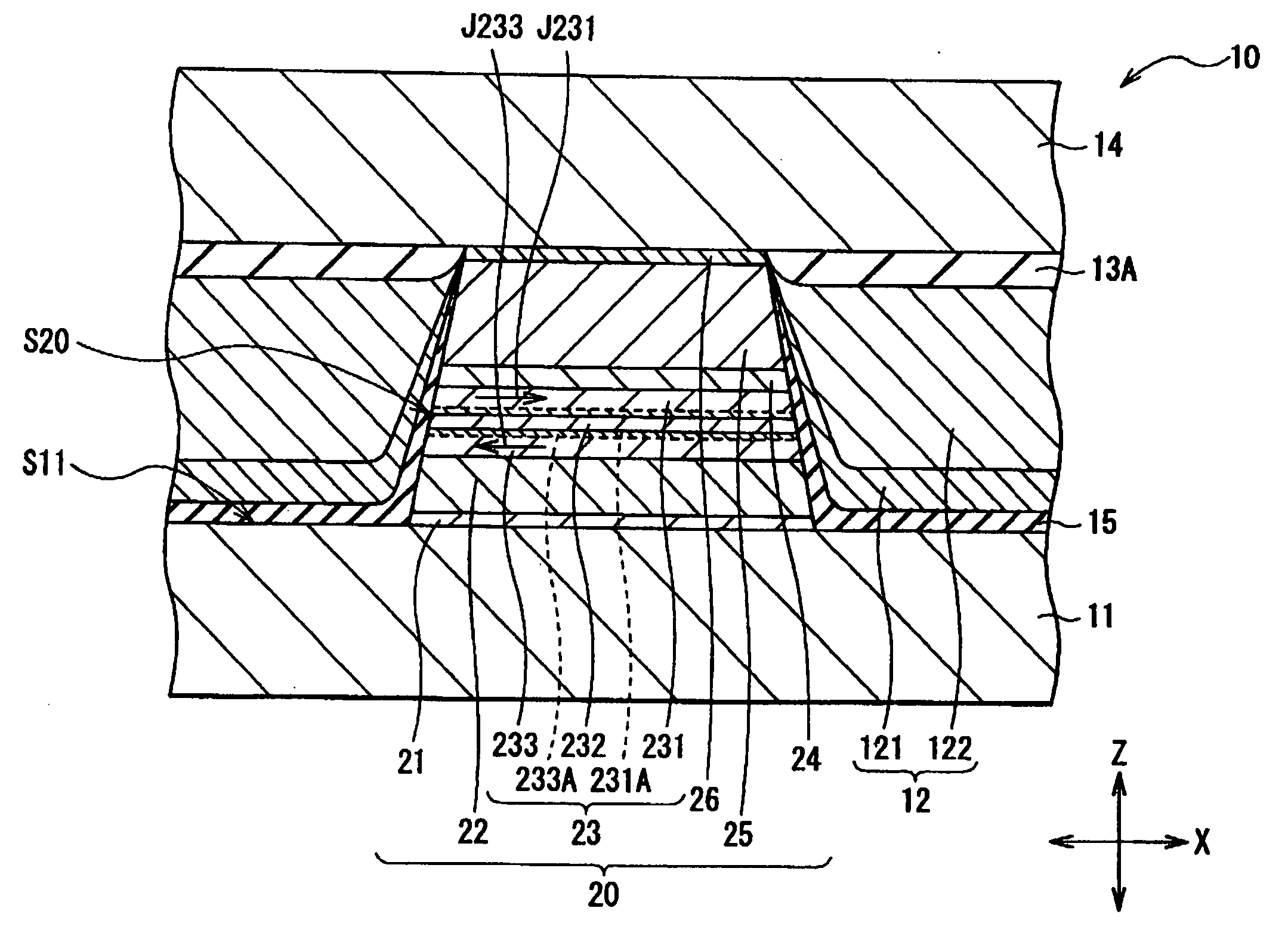
[0009] However, since the synthetic CPP-GMR element has a structure in which the magnetization directions of the first and second ferromagnetic layers are coupled anti-parallel to each other, the net moment is reduced and the magnetization directions are stabilized. On the other hand, since current is passed in the stacking direction to the SV film, a problem occurs such that part of the resistance change amount is lost due to the features of the structure. Specifically, a resistance change amount (voltage change amount) due to the GMR effect occurring between the first ferromagnetic layer and the magnetization pinned layer and a resistance change amount (voltage change amount) due to the GMR effect occurring between the second ferromagnetic layer whose magnetization direction is opposite to that of the first ferromagnetic layer and the magnetization free layer partially cancel each other. In the case of using the nonmagnetic intermediate layer made of an alloy containing ruthenium (Ru) and iron (Fe), the strength of antiferromagnetic coupling can be increased more than that in the case of using the nonmagnetic intermediate layer made of, for example, ruthenium only. However, further magnetic field stability is demanded to address higher recording density and higher packing density in future.
[0013] In the magnetoresistive device, the current sensor, the thin film magnetic head, the head gimbals assembly, the head arm assembly, and the magnetic disk apparatus of an embodiment of the present invention, the nonmagnetic intermediate film in the synthetic antiferromagnetic pinned layer is made of a ruthenium copper alloy. Consequently, the resistance value when current is passed in the stacking direction increases and spin scattering length is shortened as compared with the case where the nonmagnetic intermediate layer is made of ruthenium. It makes spins in the second magnetization pinned layer difficult to reach the magnetization free layer. As compared with the case where the nonmagnetic intermediate layer is made of a ruthenium iron alloy, the first and second magnetization pinned layers which are thicker can be antiferromagnetically coupled in magnetic fields in a wider range.
[0017] In the synthetic antiferromagnetic pinned layer of an embodiment of the present invention, the nonmagnetic intermediate layer is made of a ruthenium copper alloy. Consequently, the resistance value when current is passed in the stacking direction increases and spin scattering length is shortened as compared with the case where the nonmagnetic intermediate layer is made of ruthenium. It makes spins in the second magnetization pinned layer difficult to reach the magnetization free layer. As compared with the case where the nonmagnetic intermediate layer is made of a ruthenium iron alloy, the first and second magnetization pinned layers which are thicker can be antiferromagnetically coupled in magnetic fields in a wider range.
[0020] In the magnetic memory cell and the current sensor of an embodiment of the present invention, the nonmagnetic intermediate layer in the synthetic antiferromagnetic pinned layer is made of a ruthenium copper alloy. Consequently, the resistance value when current is passed in the stacking direction increases and spin scattering length is shortened as compared with the case where the nonmagnetic intermediate layer is made of ruthenium. It makes spins in the second magnetization pinned layer difficult to reach the magnetization free layer. As compared with the case where the nonmagnetic intermediate layer is made of a ruthenium iron alloy, the first and second magnetization pinned layers which are thicker can be antiferromagnetically coupled in magnetic fields in a wider range.
[0021] In the magnetoresistive device, the thin film magnetic head, the head gimbals assembly, the head arm assembly, the magnetic disk apparatus, the magnetic memory cell, and the current sensor of an embodiment of the present invention, the nonmagnetic intermediate layer in the synthetic antiferromagnetic pinned layer is made of a ruthenium copper alloy. As compared with the case where the nonmagnetic intermediate layer is made of ruthenium, the resistance value when current is passed in the stacking direction increases and the influence of spins in the second magnetization pinned layer on the magnetization free layer can be reduced. As a result, decrease in the resistance change amount caused by the second magnetization pinned layer can be suppressed. As compared with the case where the nonmagnetic intermediate layer is made of a ruthenium iron alloy, the first and second magnetization pinned layers which are thicker can be antiferromagnetically coupled in magnetic fields in a wider range. Thus, both increase in the resistance change amount and magnetic field stability can be achieved. Therefore, the magnetoresistive device, the thin film magnetic head, the head gimbals assembly, the head arm assembly, and the magnetic disk apparatus of an embodiment of the present invention can address higher recording density by increasing a resistance change amount as a whole while maintaining stable read operation by reducing the influence of external noise. In the magnetic memory cell of an embodiment of the present invention, while assuring stable reading / writing operations by reducing the influence of external noise, the sensitivity of the magnetoresistive film can be increased, so that it is suitable for higher integration. Further, the current sensor of the invention can measure a smaller current to be detected at high precision.
[0022] The synthetic antiferromagnetic pinned layer of an embodiment of the present invention has the nonmagnetic intermediate layer made of a ruthenium copper alloy and a pair of magnetization pinned layers sandwiching the nonmagnetic layer in the thickness direction and displaying magnetization directions pinned opposite to each other. Thus, by applying the invention to a CPP-GMR device or a magnetic tunnel junction device, a larger resistance change amount can be stably obtained.

Problems solved by technology

On the other hand, since current is passed in the stacking direction to the SV film, a problem occurs such that part of the resistance change amount is lost due to the features of the structure.

Method used


Image

  • Magnetoresistive device, thin film magnetic head, head gimbals assembly, head arm assembly, magnetic disk apparatus, synthetic antiferromagnetic magnetization pinned layer, magnetic memory cell, and current sensor
  • Magnetoresistive device, thin film magnetic head, head gimbals assembly, head arm assembly, magnetic disk apparatus, synthetic antiferromagnetic magnetization pinned layer, magnetic memory cell, and current sensor
  • Magnetoresistive device, thin film magnetic head, head gimbals assembly, head arm assembly, magnetic disk apparatus, synthetic antiferromagnetic magnetization pinned layer, magnetic memory cell, and current sensor

Examples


first embodiment

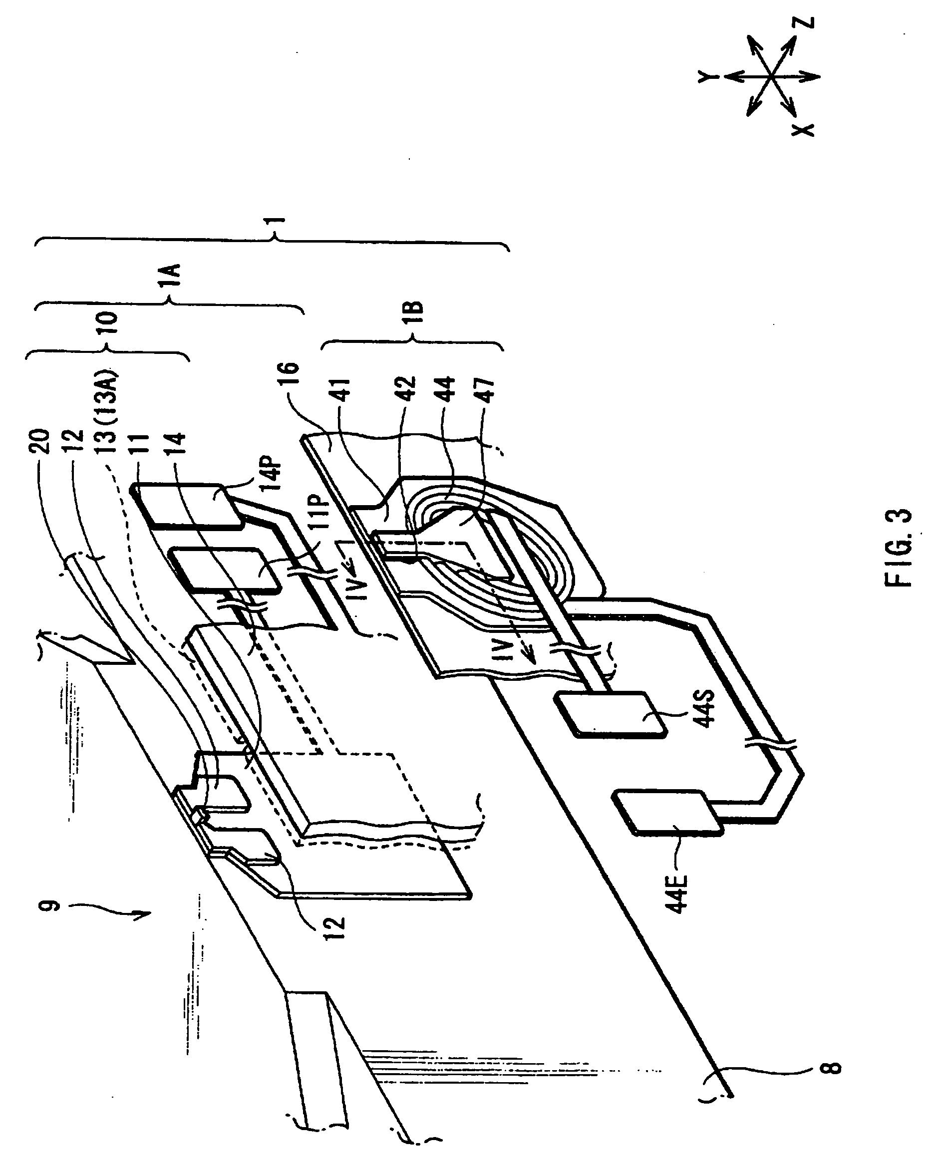
[0051] First, by referring to FIGS. 1 to 5, the configuration of a synthetic antiferromagnetic magnetization pinned layer and a magnetoresistive element, a thin film magnetic head, a head gimbals assembly, a head arm assembly, and a magnetic disk apparatus each having the synthetic antiferromagnetic magnetization pinned layer as a first embodiment of the invention will be described below.

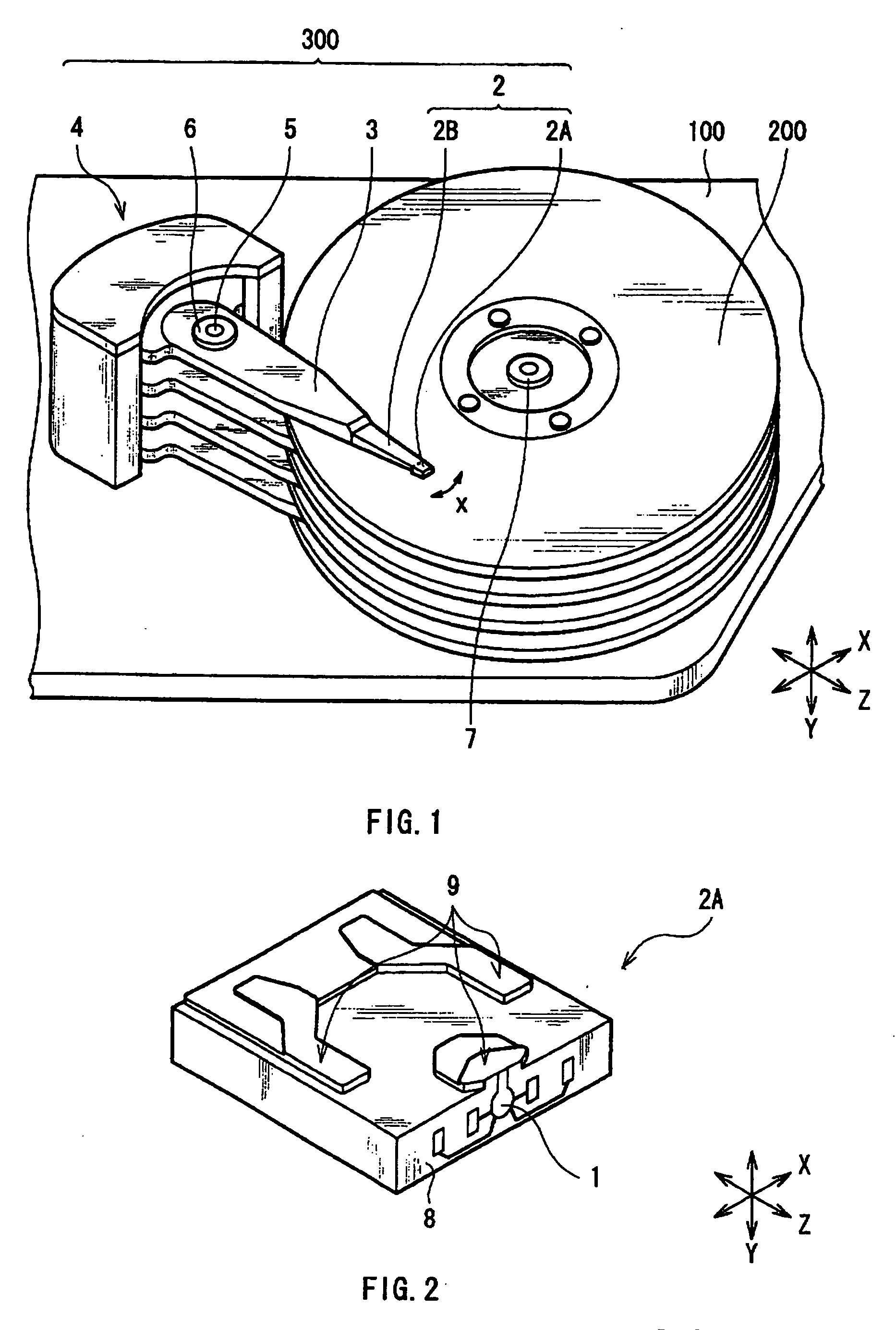
[0052]FIG. 1 is a perspective view showing the internal configuration of the magnetic disk apparatus according to the first embodiment. The magnetic disk apparatus employs, as the driving system, a CSS (Contact-Start-Stop) operating system. As shown in FIG. 1, for example, a magnetic recording medium 200 as a magnetic recording medium on which information is to be recorded and a head arm assembly (HAA) 300 for recording / reading information to / from the magnetic recording medium 200 are provided in a casing 100. The HAA 300 has a head gimbals assembly (HGA) 2, an arm 3 for supporting the base portion...

second embodiment

[0086] By referring to FIGS. 14 to 16, a magnetic memory cell and a magnetic memory cell array having the same as a second embodiment of the present invention will be described below. FIG. 14 is an enlarged plan view of a part of a magnetic memory cell array (hereinbelow, called MRAM array) in which a plurality of magnetic memory cells 101 of the second embodiment are arranged in a matrix. FIG. 15 shows a sectional structure taken along the XV-XV cut line illustrated in FIG. 14.

[0087] As shown in FIGS. 14 and 15, the MRAM array has a plurality of word lines 126 extended in the L-axis direction and arranged in the K-axis direction so as to be parallel with each other in a first level, and a plurality of bit lines 125 extended in the K-axis direction and arranged in the L-axis direction so as to be parallel with each other in a second level different from the first level. Further, one MR film 124 and one lower electrode 123 are provided to construct one magnetic memory cell 101 at ea...

third embodiment

[0095] By referring to FIGS. 17A to 17C and FIG. 18, a current sensor as a third embodiment of the present invention will now be described.

[0096]FIGS. 17A to 17C show a schematic configuration of a current sensor 210 of the third embodiment. FIG. 17A shows a plane configuration of the current sensor 210. FIG. 17B shows a sectional configuration of the current sensor 210 taken along line XVII-XVII of FIG. 17A. FIG. 17C shows an equivalent circuit corresponding to FIG. 17A. The current sensor 210 functions to detect the intensity of a current magnetic field generated by current flowing near the current sensor 210, thereby measuring the magnitude of the current.

[0097] As shown in FIG. 17A, the current sensor 210 has a configuration in which an MR film 220 and a current line 230 which is provided adjacent to the MR film 220 and through which current to be detected flows are formed over a not-shown substrate. The MR film 220 has a pinned layer whose magnetization direction is pinned in...


PUM


Abstract

An MR device includes a magnetization pinned film having a nonmagnetic intermediate layer positioned on the opposite side of a magnetization free layer while sandwiching a nonmagnetic spacer layer and made of RuCu. In the case of passing read current in the stacking direction via lower and upper electrodes, decrease in a resistance change amount caused by a second magnetization pinned layer can be suppressed. Further, a first magnetization pinned layer and the second magnetization pined layer which are thicker can be antiferromagnetically coupled to each other in magnetic fields in a wider range. Thus, both increase in the resistance change amount and magnetic field stability can be achieved. Therefore, while maintaining stable operations by reducing the influence of external noise, the invention can address higher recording density by the increase in the resistance change amount as a whole.

Description

BACKGROUND OF THE INVENTION [0001] 1. Field of the Invention [0002] The present invention relates to a synthetic antiferromagnetic pinned layer having a pair of ferromagnetic layers which are antiferromagnetic-coupled to each other with a nonmagnetic intermediate layer in between, a magnetoresistive device having the same, a thin film magnetic head, a head gimbals assembly, a head arm assembly, a magnetic disk apparatus, a magnetic memory cell, and a current sensor. [0003] 2. Description of the Related Art [0004] For reading information on a magnetic recording medium such as a hard disk, a thin film magnetic head having an MR (Magneto-Resistive) device exhibiting the MR effect is widely used. In recent years, as recording density of a magnetic recording medium is becoming higher and higher, a thin film magnetic head using a giant magneto-resistive device (GMR device) exhibiting the GMR effect is commonly used. An example of the GMR device is a spin valve (SV) type GMR device. [0005]...

Claims


Application Information

Patent Timeline
IPC IPC(8): G11B5/33G11B5/127
CPCB82Y10/00G01R33/093G11C11/16G11B5/3929G11B2005/3996G11B5/3909
Inventor MIZUNO, TOMOHITOMIYAUCHI, DAISUKE
Owner TDK CORPARATION
Learn More