Method of forming a nickel platinum silicide

a technology of nickel platinum and silicide, which is applied in the direction of basic electric elements, semiconductor/solid-state device manufacturing, electric devices, etc., can solve the problems of platinum residues and difficult etching

Inactive Publication Date: 2007-01-25
UNITED MICROELECTRONICS CORP
View PDF2 Cites 23 Cited by
  • Summary
  • Abstract
  • Description
  • Claims
  • Application Information

AI Technical Summary

Benefits of technology

[0011] It is an advantage of the present invention that the passivation layer is formed on the nickel platinum silicide, and aqua regia (the mixture of nitric acid and hydrochloric acid) is used to remove the unreacted portions of the nickel platinum alloy layer after the formation of the passivation layer. As a result, the issues of platinum residues and silicide damage caused by a reaction between the aqua regia and the nickel platinum silicide can be effectively prevented.
[0012] These and other objects of the claimed invention will be apparent to those of ordinary skill in the art with reference to the following detailed description of the preferred embodiments illustrated in the various drawings.

Problems solved by technology

Since the nickel silicide NiSi2 has low thermal stability, it's possible that nickel may penetrate through the interface between metal and silicon down to the gate electrode to cause spiking effect, or it's possible that nickel may laterally diffuse to the channel region to cause nickel piping effect.
However, platinum also has the property of being difficult to etch, which results in platinum residues issues during the removal of the unreacted metal layer.

Method used


Image

  • Method of forming a nickel platinum silicide
  • Method of forming a nickel platinum silicide
  • Method of forming a nickel platinum silicide

Examples


Embodiment Construction

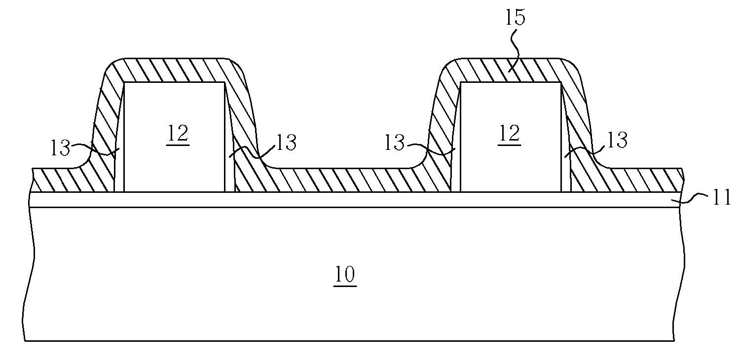
[0017] Referring to FIGS. 3-7, FIGS. 3-7 are schematic diagrams of a method of forming a nickel platinum silicide according to the present invention. As shown in FIG. 3, a substrate 10, such as a silicon substrate, is provided. An oxide layer 111 is formed on the substrate 10, at least one silicon device 12, such as a polysilicon gate electrode, is formed on the oxide layer 11, and a spacer 13 is formed on either side of the silicon device 12. In a better embodiment of the present invention, the silicon device 12 is not limited to the gate electrode. The silicon device 12 may include a source / drain region formed on the substrate 10, or include both of the gate electrode and the source / drain region.

[0018] As shown in FIG. 4, an alloy layer 15, such as a nickel platinum alloy layer, is formed on the substrate 10 and contacts to the exposed surface of the silicon device 12. In other embodiments of the present invention, the alloy layer 15 may be other alloy having platinum, and the pe...


PUM

PropertyMeasurementUnit
thicknessaaaaaaaaaa
resistanceaaaaaaaaaa
electrical resistivityaaaaaaaaaa

Abstract

A substrate having at least one silicon device is provided. A nickel platinum alloy layer is formed on the substrate. A rapid thermal process is performed to react the nickel platinum alloy layer with the silicon device to produce a nickel platinum silicide. A passivation layer is formed on the nickel platinum silicide followed by using a solution consisting of nitric acid and hydrochloric acid to remove unreacted portions of the nickel platinum alloy layer.

Description

BACKGROUND OF THE INVENTION [0001] 1. Field of the Invention [0002] The present invention relates to a method of forming a silicide, and more particularly, to a method of forming a silicide without leaving platinum residues. [0003] 2. Description of the Prior Art [0004] A silicide layer is currently used in the fabrication of metal-oxide-semiconductor (MOS) transistors on a wafer. For example, the silicide layer is often formed on the surface of a gate electrode. The silicide layer provides a good ohmic contact at the interface of the gate electrode and a subsequently formed metal layer, thus reducing resistance of the gate electrode. Among silicide constituents, nickel silicide is considered important to the development of manufacturing processes in the 65 nm MOSFET technology or less because of the characteristics including low electrical resistivity, low silicon consumption, good resistance behavior in narrow lines, and low processing temperature. [0005] A conventional method of ...

Claims


Application Information

Patent Timeline
Patent Type & Authority Applications(United States)
IPC IPC(8): H01L21/44
CPCH01L21/28518H01L21/28052
Inventor HSIEH, CHAO-CHINGCHIANG, YI-YIINGHUNG, TZUNG-YUCHEN, YI-WEICHANG, YU-LAN
Owner UNITED MICROELECTRONICS CORP
Why Eureka
Try Eureka