Etch chamber with dual frequency biasing sources and a single frequency plasma generating source

a plasma generating source and etch chamber technology, applied in the direction of electrical discharge tubes, basic electric elements, electrical equipment, etc., can solve the problems of limited deep trench process and long exposure of etchants to etchants, and achieve the effects of improving plasma control, enhancing plasma density control, and increasing process window

Inactive Publication Date: 2007-01-25
CHEN JIN YUAN +2
View PDF68 Cites 31 Cited by
  • Summary
  • Abstract
  • Description
  • Claims
  • Application Information

AI Technical Summary

Benefits of technology

[0007] The present invention provides an etch chamber that is driven with three RF frequencies: one frequency for establishing and maintaining a plasma, and two frequencies for biasing a biasing element (e.g., wafer pedestal). Such triple frequency use provides improved plasma control that increases the process window for an etch process. Enhancing control of plasma density and ion energy improves the coverage of more etching applications and provides a wider window of processing.

Problems solved by technology

However, during “deep trench etching”, the wafer may be exposed to the etchants for a long duration.
That is, the deep trench processes are limited by the selectivity between the material of the protective mask and the material to be etched, where the higher the selectivity, the deeper the trench may be etched.

Method used


Image

  • Etch chamber with dual frequency biasing sources and a single frequency plasma generating source
  • Etch chamber with dual frequency biasing sources and a single frequency plasma generating source
  • Etch chamber with dual frequency biasing sources and a single frequency plasma generating source

Examples


Embodiment Construction

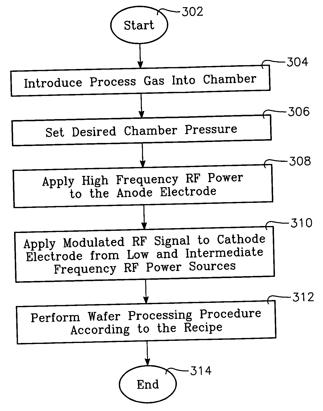
[0017] One application of the present invention provides an apparatus for performing high aspect ratio deep trench etching. In particular, a processing chamber is equipped with dual frequency biasing sources and a single frequency plasma generating source. A wafer to be processed is secured on a support pedestal in the chamber. The single frequency plasma generating source is coupled to a plasma generating element disposed over the wafer to be processed, while a pair of biasing sources having different frequencies are coupled to the support pedestal, such that the support pedestal serves as a biasing element.

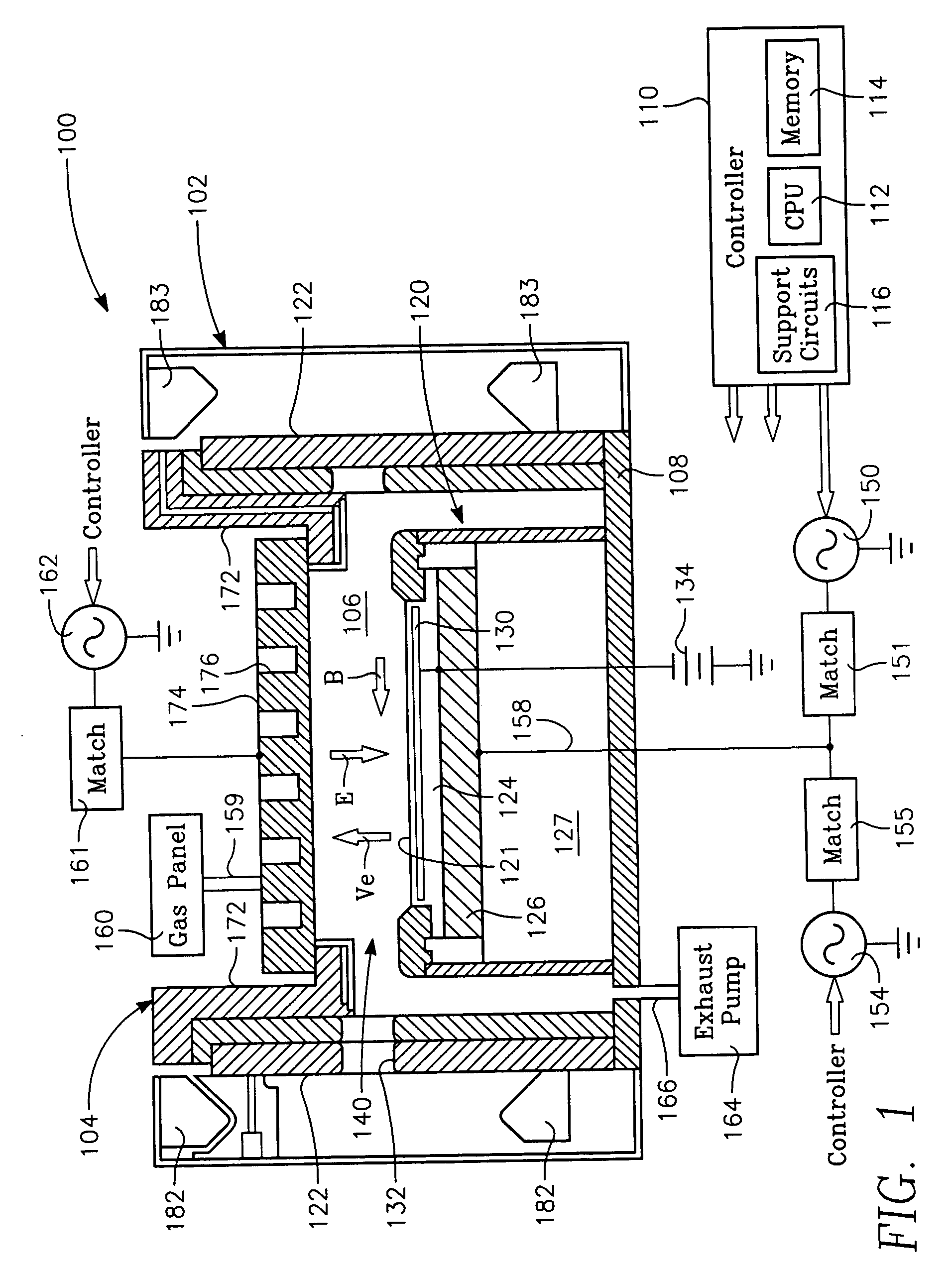
[0018]FIG. 1 depicts a cross sectional view of a first embodiment of a dual frequency bias plasma chamber system 100 of the present invention. Specifically, FIG. 1 depicts an illustrative chamber system (system) 100 that can be used in high aspect ratio trench formation. The system 100 generally comprises a chamber body 102 and a lid assembly 104 that defines an evacuable chamb...


PUM


Abstract

A method and apparatus for selectively controlling a plasma in a processing chamber during wafer processing. The method includes providing process gasses into the chamber over a wafer to be processed, and providing high frequency RF power to a plasma generating element and igniting the process gases into the plasma. Modulated RF power is coupled to a biasing element, and wafer processing is performed according to a particular processing recipe. The apparatus includes a biasing element disposed in the chamber and adapted to support a wafer, and a plasma generating element disposed over the biasing element and wafer. A first power source is coupled to the plasma generating element, and a second power source is coupled to the biasing element. A third power source is coupled to the biasing element, wherein the second and third power sources provide a modulated signal to the biasing element.

Description

CROSS REFERENCE TO RELATED APPLICATION [0001] This patent application is a continuation of U.S. patent application Ser. No. 10 / 342,575 filed Jan. 14, 2003, which claims the benefit of U.S. Provisional Application, Ser. No. 60 / 402,291, filed Aug. 9, 2002, the contents of which are incorporated by reference herein.FIELD OF THE INVENTION [0002] Embodiments of the invention generally relate to semiconductor wafer processing, and more particularly, to etch and plasma related integrated circuit manufacturing processes and related hardware. BACKGROUND OF THE INVENTION [0003] Semiconductor fabrication wafer process chambers employing plasma to perform etching and deposition processes utilize various techniques to control plasma density and acceleration of plasma components. For example, magnetically-enhanced plasma chambers employ magnetic fields to increase the density of charged particles in the plasma, thereby further increasing the rate of plasma-enhanced deposition and etching processe...

Claims


Application Information

Patent Timeline
Patent Type & Authority Applications(United States)
IPC IPC(8): H01L21/302H01J37/32
CPCH01J37/32706H01J37/321
Inventor CHEN, JIN-YUANHOOSHDARAN, FRANK F.PODLESNIK, DRAGAN V.
Owner CHEN JIN YUAN
Why Eureka
Try Eureka