Method, program, and apparatus for designing layout of semiconductor integrated circuit

a technology for integrated circuits and layouts, applied in the direction of cad circuit design, program control, instruments, etc., can solve the problems of increasing the number of violations of design rules occurring at the connection point between wires and pins of standard cells, the influence of wiring delay time is no longer negligible in the design of a semiconductor integrated circuit, and the number of violations of design rules has increased. , to achieve the effect of suppressing violations, reducing the density of the route at the wire connection poin

Inactive Publication Date: 2007-01-25
PANASONIC CORP
View PDF3 Cites 17 Cited by
  • Summary
  • Abstract
  • Description
  • Claims
  • Application Information

AI Technical Summary

Benefits of technology

[0038] As described above, according to the present invention, layout information sets on respective standard cells in a semiconductor integrated circuit are each assigned one or more parameters, each of which indicates the probability of occurrence of violations of design rules at a connection point between a corresponding pin and a wire in the standard cells. And according to the assigned parameters, global routing is designed in such a manner that as the probab

Problems solved by technology

In recent years, as microscaling of semiconductor fabrication processes has progressed, the influence of wiring delay time is no longer negligible in designing a semiconductor integrated circuit.
However, since capacitance between wires has been increasing due to the microscaling of the fabrication processes, the wiring delay time has become dominant.
Nevertheless, as the size of standard cells has been decreased, the number of violations of design rules occurring a

Method used


Image

  • Method, program, and apparatus for designing layout of semiconductor integrated circuit
  • Method, program, and apparatus for designing layout of semiconductor integrated circuit
  • Method, program, and apparatus for designing layout of semiconductor integrated circuit

Examples


Embodiment Construction

[0043] Hereinafter, preferred embodiments of the present invention will be described in detail with reference to the accompanying drawings.

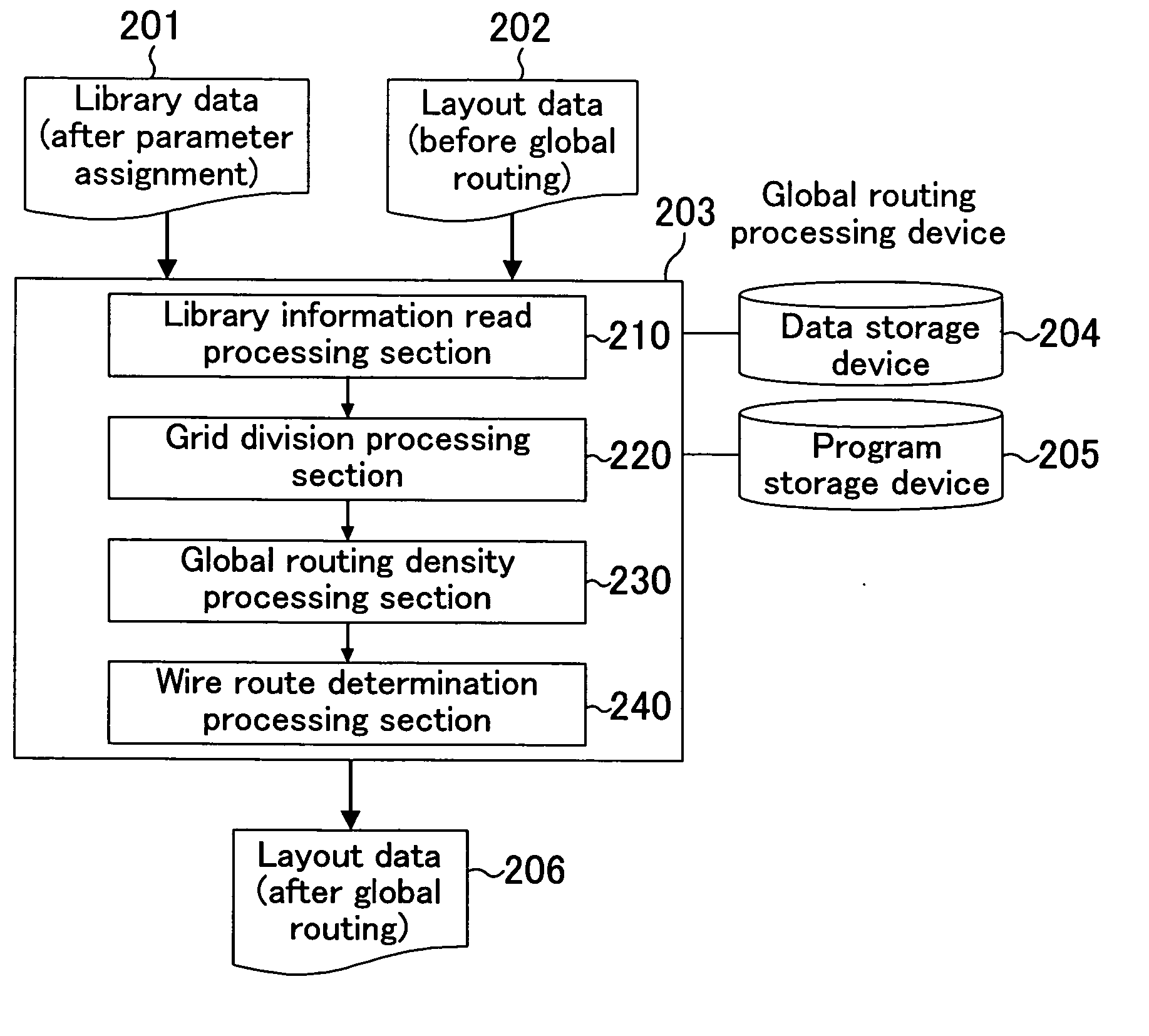
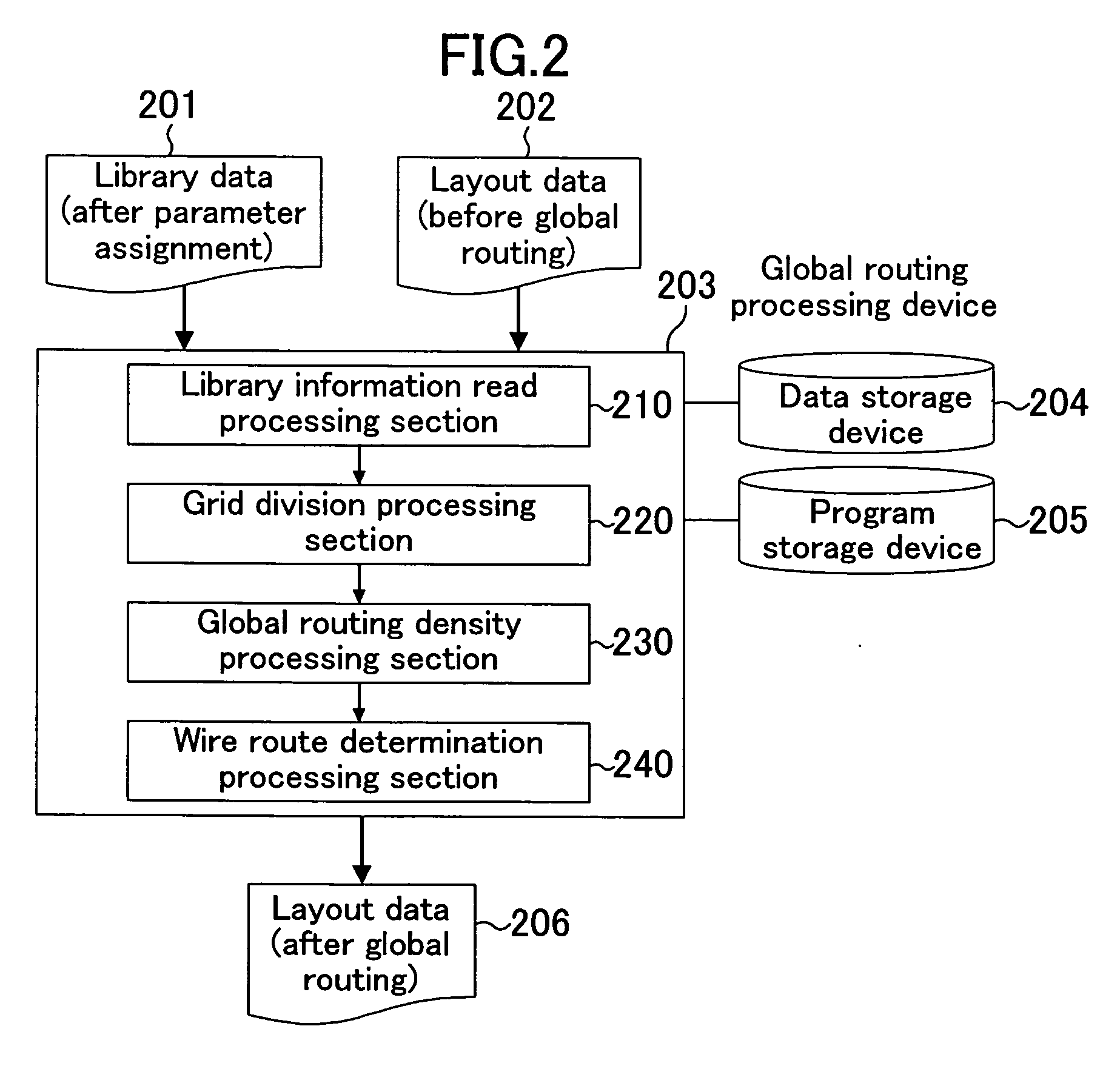
[0044] First of all, the entire process flow will be described.

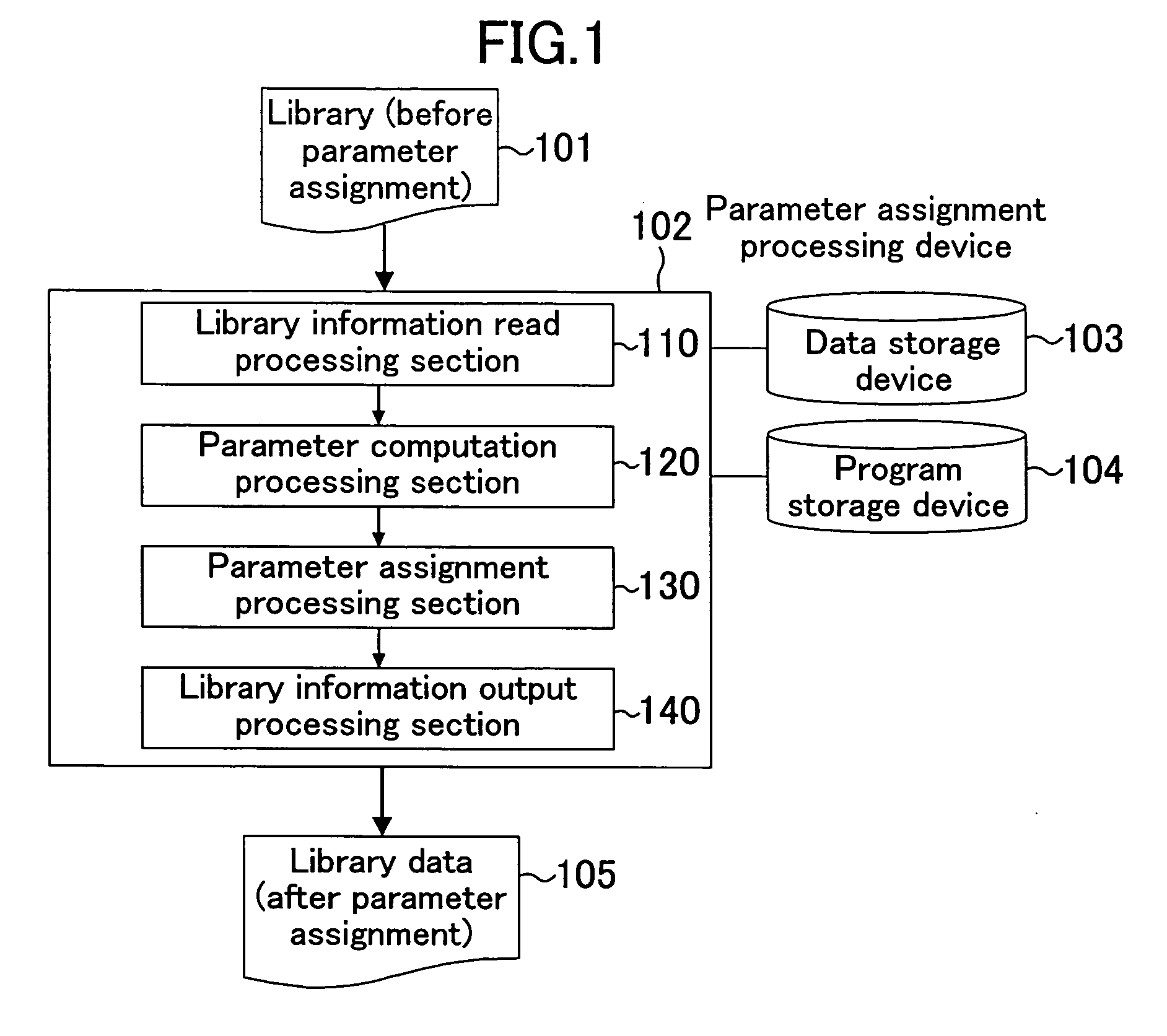
[0045] The entire process flow is broadly divided into two processes: a process for assigning parameters to information about standard cells and a process for carrying out global routing. A configuration for performing these processes is shown in FIGS. 1 and 2. FIG. 1 shows part of the configuration for performing the parameter assigning process, while FIG. 2 shows part of the configuration for carrying out the global routing process.

[0046] In FIG. 1, the reference numeral 101 denotes library in which information sets on standard cells before parameter assignment are stored. The reference numeral 102 refers to a parameter assignment processing device for receiving an information set on a standard cell stored in the library 101 and performing the parameter assignment process for tha...


PUM


Abstract

In a method for designing a layout for an LSI, library data, which is information on a standard cell with an assigned parameter or parameters each indicating the probability of occurrence of violations of design rules at a pin connection point, is read into a library information read section in a global routing processing device. And in a global routing density processing section and a wire route determination processing section, the density of global routes that pass above a chip area divided into a plurality of portions in a grid pattern by a grid division processing section is set according to the parameters, so that the density of routes at pin connection points where the probability of occurrence of violations of design rules is high becomes low. Therefore, the global routing is carried out in such a manner that occurrence of violations of design rules at the pin connection points are prevented as much as possible.

Description

CROSS-REFERENCE TO RELATED APPLICATION [0001] This Non-provisional application claims priority under 35 U.S.C. § 119(a) on Patent Application No. 2005-208531 filed in Japan on Jul. 19, 2005, the entire contents of which are hereby incorporated by reference.BACKGROUND OF THE INVENTION [0002] The present invention relates to an automatic layout method, program, and apparatus for determining global routes with consideration given to wire closure, when a semiconductor integrated circuit is designed. [0003] In recent years, as microscaling of semiconductor fabrication processes has progressed, the influence of wiring delay time is no longer negligible in designing a semiconductor integrated circuit. Signal delay time is broadly divided into cell delay time and wiring delay time. Previously, the cell delay time was predominant and it was thus easy to estimate signal delay in a semiconductor integrated circuit in a step for designing logic circuits. However, since capacitance between wires...

Claims


Application Information

Patent Timeline
IPC IPC(8): G06F17/50
CPCG06F17/5068G06F30/39
Inventor KADOTA, TADAFUMI
Owner PANASONIC CORP
Why Eureka
Try Eureka