Wafer holder, heater unit having the wafer holder, and wafer prober having the heater unit

a technology of heater unit and heater, which is applied in the direction of electrical equipment, other accessories, packaging, etc., can solve the problems of long time between the temperature of the heater contained in the chuck and the contact failure between the wafer and the ground electrode, and improve the throughput, so as to prevent the contact failure, prevent the deformation of the chuck, and prevent the effect of temperature increas

Inactive Publication Date: 2007-02-01
SUMITOMO ELECTRIC IND LTD
View PDF4 Cites 35 Cited by
  • Summary
  • Abstract
  • Description
  • Claims
  • Application Information

AI Technical Summary

Benefits of technology

[0015] In view of the situations of the conventional art as described above, an object of the present invention is to provide a wafer holder capable of effectively preventing contact failure with a wafer, with deformation of a chuck top being small even under high load. A further object is to provide a wafer holder capable of preventing temperature increase in a driving system of the wafer holder, when a semiconductor wafer having minute circuitry requiring particularly high accuracy is mounted on a chuck top and heated. A still further object is to provide a heater unit including the wafer holder described above and a wafer prober including the heater unit.

Problems solved by technology

As described above, the wafer mounted on the chuck top is pressed to the probe card with a strong force of several tens to several hundreds kgf, and therefore, when the heater is thin, the heater would possibly be deformed, resulting in contact failure between the wafer and the ground electrode.
As a result, it takes long time to increase and decrease the temperature of the heater contained in the chuck top, which is a significant drawback in improving the throughput.
As recent chips come to have higher outputs, it is possible that a chip generates considerable heat during measurement of electric characteristics, and in some situations, the chip might be broken by self-heating.
There is a problem, however, that when the wafer is heated to a prescribed temperature, that is, to about 100 to 200° C., the heat is transferred to the driving system, and metal components forming the driving system thermally expand, degrading positional accuracy.
This is a cause of a contact failure made more likely during an inspection of a semiconductor chip having a particularly minute circuitry.
Further, along with the increase in load at the time of probing, rigidity of the prober itself mounting the wafer has come to be required.
Specifically, when the wafer prober itself deforms because of the load at the time of probing, uniform contact of the pins of probe card with the wafer would fail and inspection becomes impossible, or in the worst case, the wafer would be broken.
In order to suppress deformation of the prober, the prober has been made larger and its weight has been increased, posing a problem that the increased weight adversely influences the accuracy of the driving system.
Further, as the prober is made larger, the time for heating and cooling the prober becomes extremely long, posing another problem of lower throughput.
The former approach has a problem that cooling rate is slow, as it is air-cooling.
The latter approach also has a problem that, as the cooling plate is metal and the pressure of the probe card directly acts on the cooling plate at the time of probing, it is susceptible to deformation.
Further, in the prober, stress generated at the time of probing results in a load on the chuck top, causing deformation.
When the deformation involves large deflection, state of contact between the large number of probe pins attached to the probe card and the wafer may vary and errors may possibly occur at the time of measurement, posing a problem that accurate evaluation becomes impossible.

Method used


Image

  • Wafer holder, heater unit having the wafer holder, and wafer prober having the heater unit
  • Wafer holder, heater unit having the wafer holder, and wafer prober having the heater unit
  • Wafer holder, heater unit having the wafer holder, and wafer prober having the heater unit

Examples


example 1a

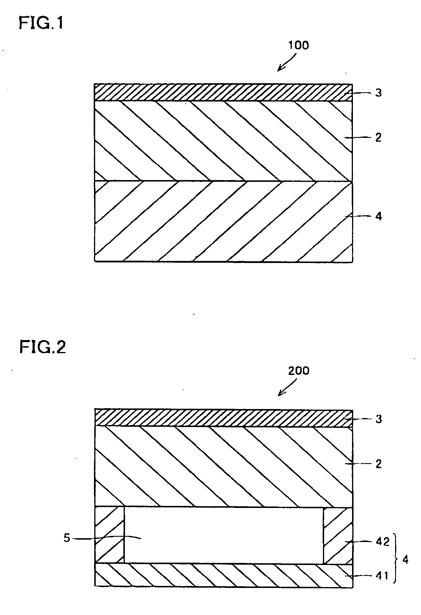
[0157] A wafer holder 300 having the structure shown in FIG. 4 with an integral type supporter 4 was fabricated. As chuck top 2, an Si—SiC substrate having the diameter of 310 mm and thickness of 15 mm was prepared. On one surface of the substrate, a concentrical trench for vacuum chucking a wafer and a through hole were formed, and nickel plating was applied as chuck top conductive layer 3, and thus the wafer-mounting surface was formed. Thereafter, the wafer-mounting surface was polished to attain surface roughness Ra of 0.02 μm. Further, the contact surface between chuck top 2 and supporter 4 was polished and finished such that the amount of warp of the entire body was set to 10 μm and variation in thickness from the wafer-mounting surface to the contact surface with supporter 4 was set to 45 μm, and thus, chuck top 2 was completed.

[0158] Next, as supporter 4, a cylindrical plate of mullite-alumina composite having the diameter of 310 mm and the height of 40 mm was prepared. The...

example 2a

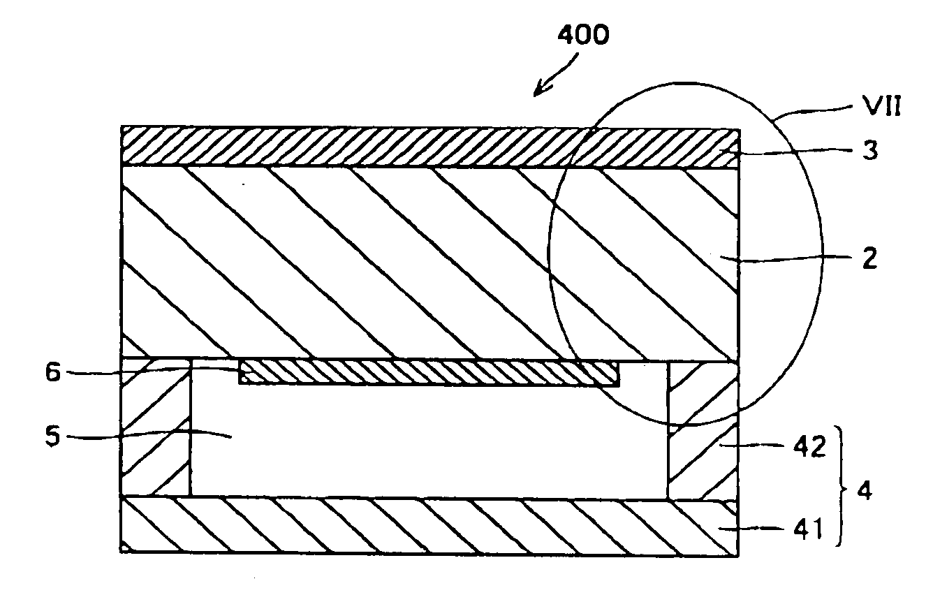
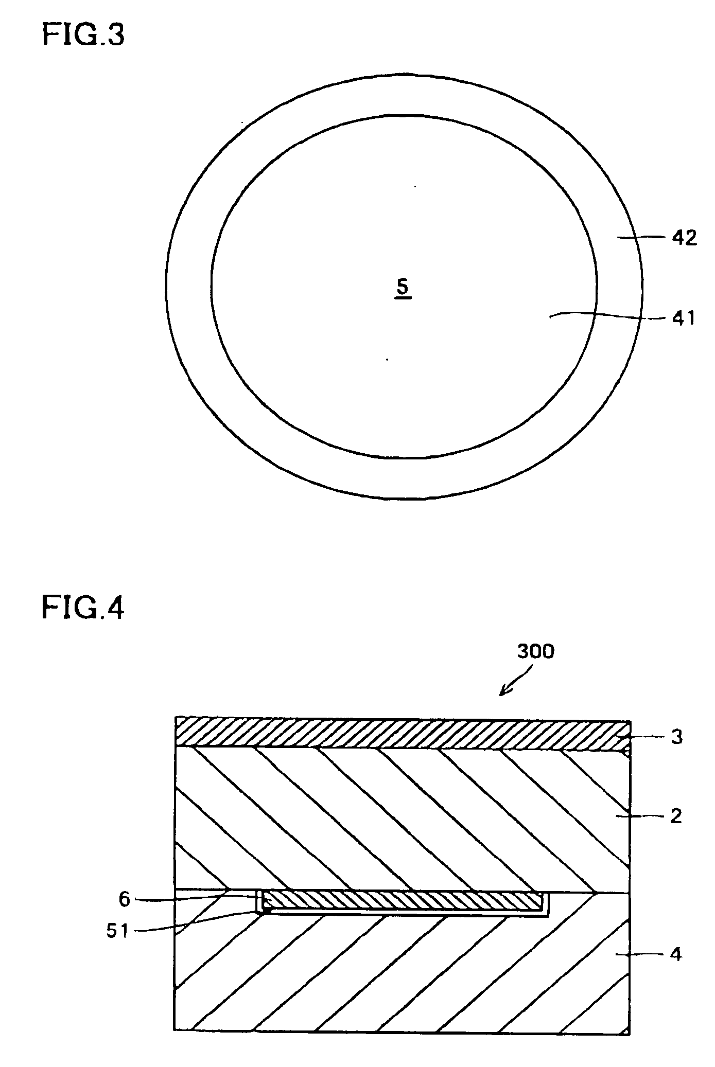
[0164] A wafer holder 400 having a separate type supporter 4 with base portion 41 and circular tube portion 42 such as shown in FIG. 5 was fabricated. First, chuck top 2 was fabricated in the similar manner as in Example 1A except that the variation in thickness of chuck top 2 from the wafer-mounting surface to the contact surface with supporter 4 was set to 46 μm.

[0165] Further, as components of supporter 4, a circular tube portion formed of a mullite-alumina composite having the diameter of 310 mm, radial thickness of 10 mm and height of 30 mm, and a base portion formed of a mullite-alumina composite having the diameter of 310 mm and thickness of 15 mm were prepared. The circular tube portion and the base portion were polished and finished such that the variation in thickness of circular tube portion 42 from the contact surface with the chuck top 2 to the contact surface with the base portion 41 attained to 22 μm, and the variation in thickness of base portion 41 from the bottom ...

example 3a

[0167] A wafer holder 400 having a separate type supporter 4 with base portion 41 and circular tube portion 42 such as shown in FIG. 5 was fabricated. Here, wafer holder 400 having a separate type supporter 4 such as shown in FIG. 5 was fabricated in the similar manner as Example 2A except that the variation in thickness of chuck top 2 from the wafer-mounting surface to the contact surface with supporter 4 was set to 9 μm, the variation in thickness of circular tube portion 42 from the contact surface with the chuck top 2 to the contact surface with the base portion 41 was set to 5 μm, and the variation in thickness of base portion 41 from the bottom surface to the contact surface with circular tube portion 42 was set to 4 μm. At this time, the variation in thickness of supporter 4 from the bottom surface to the contact surface with chuck top 2 was 10 μm.

[0168] The obtained wafer holder was mounted on a wafer prober, and semiconductor wafers were inspected continuously for 10 hours...


PUM


Abstract

A wafer holder hardly deformable under high load and capable of effectively preventing a contact failure with a wafer and further capable of preventing temperature increase of a driving system of a wafer prober is provided. In a wafer holder having a chuck top and a supporter, variation in thickness of the chuck top from a wafer-mounting surface to a contact surface with the supporter, and variation in thickness of the supporter from a bottom surface to a contact surface with the chuck top are both set to at most 50 μm. When the supporter is of a structure having a circular tube portion and a base portion separate from each other, variation in thickness of the circular tube portion from a contact surface with the chuck top to a contact surface with the base portion, and variation in thickness of the base portion from a bottom surface to a contact surface with the circular tube portion are preferably both set to at most 25 μm.

Description

BACKGROUND OF THE INVENTION [0001] 1. Field of the Invention [0002] The present invention relates to a wafer holder used for a wafer prober for inspecting electric characteristics of a semiconductor wafer by mounting and fixing the wafer on a wafer-mounting surface and pressing a probe card on the wafer, as well as to a heater unit including the wafer holder and a wafer prober including the heater unit. [0003] 2. Description of the Background Art [0004] Conventionally, in a process for inspecting a semiconductor wafer, a semiconductor wafer (wafer) as an object of processing has been subjected to heat treatment (that is, burn-in). Specifically, by heating the wafer to a temperature higher than the normal temperature of use, degradation of a possibly defective semiconductor chip is accelerated and the defective chip is removed, in order to prevent defects after shipment. In the burn-in process, after semiconductor circuits are formed on the semiconductor wafer and before the wafer is...

Claims


Application Information

Patent Timeline
Patent Type & Authority Applications(United States)
IPC IPC(8): B65D85/00
CPCH01L21/68757H01L21/67103
Inventor ITAKURA, KATSUHIRANATSUHARA, MASUHIROAWAZU, TOMOYUKINAKATA, HIROHIKOSHINMA, KENJI
Owner SUMITOMO ELECTRIC IND LTD
Why Eureka
Try Eureka