Virtual body-contacted trigate

a tri-gate, virtual body technology, applied in the direction of semi-conductor devices, basic electric elements, electrical equipment, etc., can solve the problems of reducing size, lack of electrical threshold voltage (v), and reducing siz

Inactive Publication Date: 2007-02-01
GLOBALFOUNDRIES INC
View PDF22 Cites 18 Cited by
  • Summary
  • Abstract
  • Description
  • Claims
  • Application Information

AI Technical Summary

Benefits of technology

[0006] In view of the foregoing, an embodiment of the invention provides a field effect transistor (FET) comprising a substrate; a silicon germanium (SiGe) layer over the substrate; a semiconductor layer over and adjacent to the SiGe layer; an insulating layer adjacent to the substrate, the SiGe layer, and the semiconductor layer; a pair of first gate structures adjacent to the insulating layer; and a second gate structure over the insulating layer. Preferably, the insulating layer is adjacent to a side surface of the SiGe layer and an upper surface of the semiconductor layer, a lower surface of the semiconductor layer, and a side surface of the semiconductor layer. Preferably, the SiGe layer comprises carbon. Preferably, the pair of first gate structures are substantially transverse to the second gate structure. Additionally, the pair of first gate structures are preferably encapsulated by the insulating layer.

Problems solved by technology

Trigate devices have been shown in HOT but generally lack a means of electrical threshold voltage (Vt) adjustment.
Moreover, as devices physically diminish in size, threshold voltage control by doping generally becomes increasingly ineffective due to dopant fluctuations in the individual devices.
Additionally, Vt control is becoming a major barrier to the further scaling of CMOS devices.

Method used


Image

  • Virtual body-contacted trigate
  • Virtual body-contacted trigate
  • Virtual body-contacted trigate

Examples


first embodiment

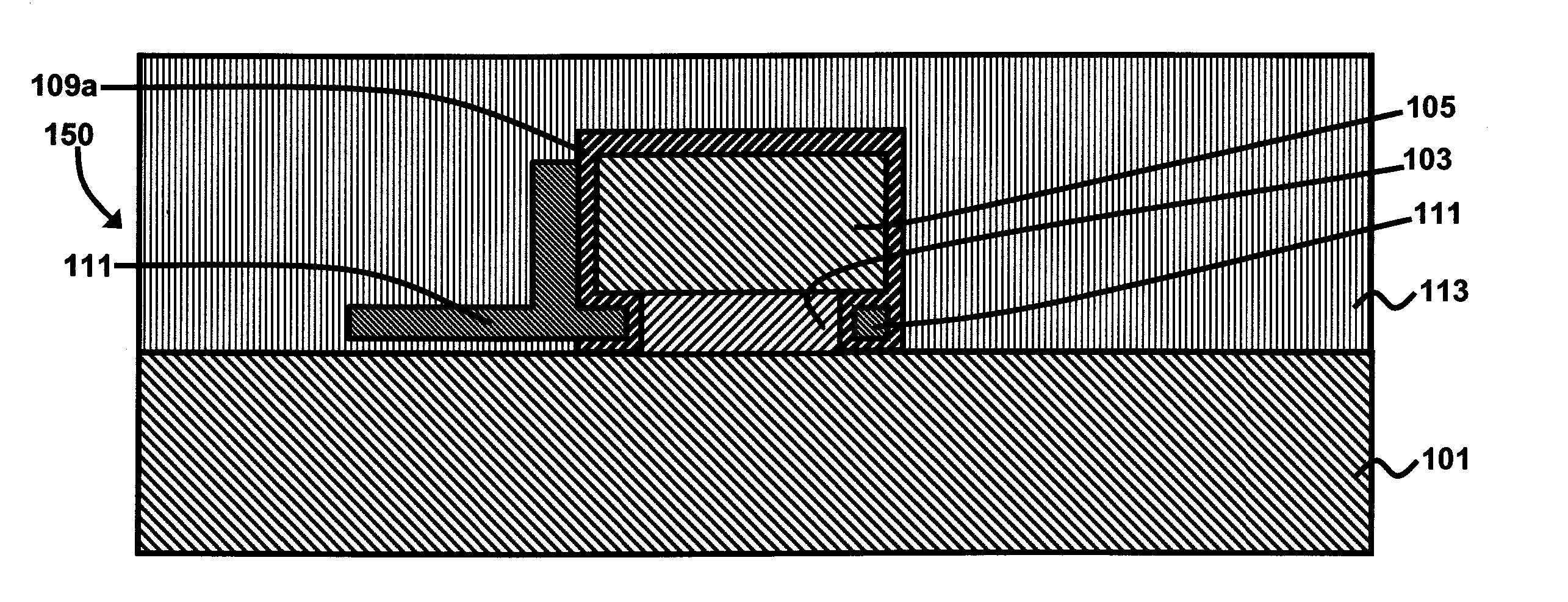
[0026] Accordingly, the invention provides for the isolation of bulk trigate fins 105 from the substrate 101 with (1) well-controlled fin height, which is key to Vt control in the trigate, (2) well-controlled isolation of the bulk parasitic channel (not shown), and (3) the opportunity to selectively “float” the body of the trigate device by the application of a cut-off voltage to the isolation gate 113.

[0027] In the second embodiment of the invention illustrated in FIGS. 9 through 14, the same base substrate as was provided in the first embodiment including the wafer 101, SiGe layer 103, and silicon layer 105 is formed. Thereafter, as shown in FIG. 9, a first mask 106a is patterned over the silicon layer 105 to expose a portion of the underlying silicon layer 105. A deep implant well region 108 is formed using well-known ion implantation techniques. For example, the well region 108 may serve as the eventual p-well region of the device. Depending on the ion implantation parameters, t...

second embodiment

[0030] the invention provides a structure and method capable of providing the electrical setting of the Vt in a trigate CMOS device 160 in a manner that provides for the precise control of the fin height. The height of the fin 105, 205 is given by the thickness of silicon region 105, which is enabled by the selective etch / oxidation properties of the SiGe layer 103. Furthermore, for trigate structures the ratio of the width of the fin 105, 205 to the height of the fin 105, 205 is in a ratio preferably between 2:1 and 1:2. Furthermore, voltage can be applied to the retrograde well 108 to alter or control the Vt.

third embodiment

[0031] the invention is illustrated in FIGS. 15 through 23. A hybrid SOI base substrate is provided comprising a silicon substrate 101 with first surface orientation, a buried oxide region, 103, and silicon region 105 with second surface orientation. Preferably, the substrate 101 will have a surface orientation of {100} and the second silicon region 105 will have surface orientation of {110}, although the opposite, and other combinations are possible. Thereafter, as shown in FIG. 15, a silicon dioxide (SiO2) layer 100 and a silicon nitride (Si3N4) layer 106 are sequentially deposited over the silicon layer 105. SiO2 layer 100 preferably has an approximate thickness between 5 and 50 nm while Si3N4 layer 106 preferably has an approximate thickness between 5 and 50nm. Next, a selective etching process is performed, as shown in FIG. 16, to remove portions of the buried oxide layer 103, silicon layer 105, SiO2 layer 100, and Si3N4 layer 106, thereby exposing portions of the underling sub...


PUM


Abstract

A field effect transistor (FET) and method of forming the FET comprises a substrate; a silicon germanium (SiGe) layer over the substrate; a semiconductor layer over and adjacent to the SiGe layer; an insulating layer adjacent to the substrate, the SiGe layer, and the semiconductor layer; a pair of first gate structures adjacent to the insulating layer; and a second gate structure over the insulating layer. Preferably, the insulating layer is adjacent to a side surface of the SiGe layer and an upper surface of the semiconductor layer, a lower surface of the semiconductor layer, and a side surface of the semiconductor layer. Preferably, the SiGe layer comprises carbon. Preferably, the pair of first gate structures are substantially transverse to the second gate structure. Additionally, the pair of first gate structures are preferably encapsulated by the insulating layer.

Description

BACKGROUND OF THE INVENTION [0001] 1. Field of the Invention [0002] The embodiments of the invention generally relate to semiconductor devices, and, more particularly, to a field effect transistor (FET) device. [0003] 2. Description of the Related Art [0004] Hybrid orientation technology (HOT) provides surfaces for PFET inversion layers and surfaces for NFET inversion layers. A low-cost means of achieving HOT technology results in the device bodies of one type of FET being isolated by oxide (silicon on insulator (SOI)) and the other being physically connected to the bulk wafer. Trigate devices have been shown in HOT but generally lack a means of electrical threshold voltage (Vt) adjustment. Setting the height of the fin in a trigate device on bulk silicon is generally critical because the design requires that the width and the height be controlled to assure full depletion and controlled short-channel effects. [0005] Trigate technology has been proposed for extending scaling of compl...

Claims


Application Information

Patent Timeline
Patent Type & Authority Applications(United States)
IPC IPC(8): H01L29/12H01L21/84
CPCH01L29/42384H01L29/66795H01L29/78687H01L29/78615H01L29/785H01L29/772
Inventor ANDERSON, BRENT A.BREITWISCH, MATTHEW J.NOWAK, EDWARD J.RAINEY, BETHANN
Owner GLOBALFOUNDRIES INC
Why Eureka
Try Eureka