

Electron emission material and electron emission panel having the same
a technology of electron emission panel and electron emission material, which is applied in the direction of discharge tube luminescnet screen, discharge tube main electrode, tube with electrostatic control, etc., can solve the problems of short lifetime of electron emission material, small electron emission, and unsatisfactory applications of carbon nanotube feds
- Summary
- Abstract
- Description
- Claims
- Application Information
AI Technical Summary
Benefits of technology
Problems solved by technology
Method used
Image

Examples
first embodiment
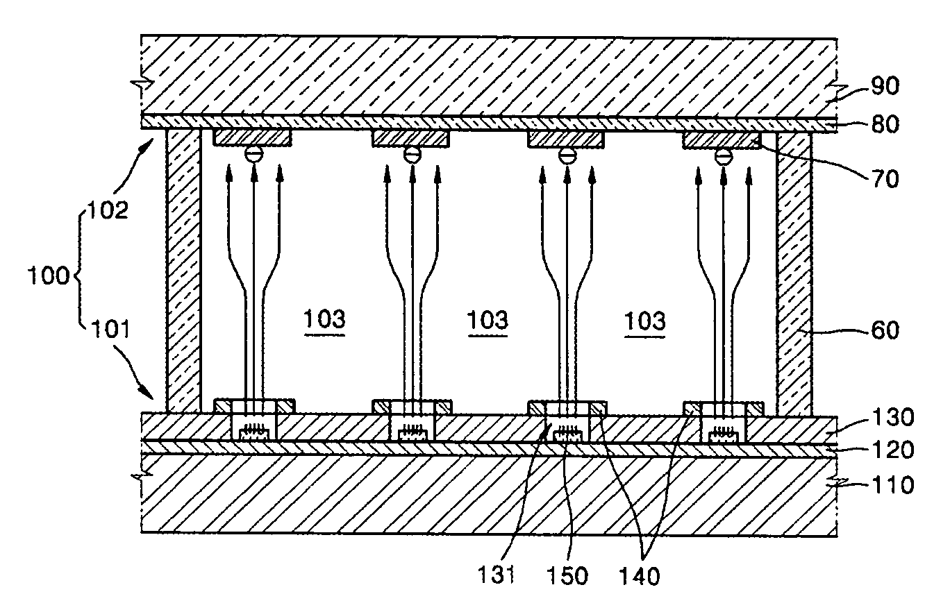
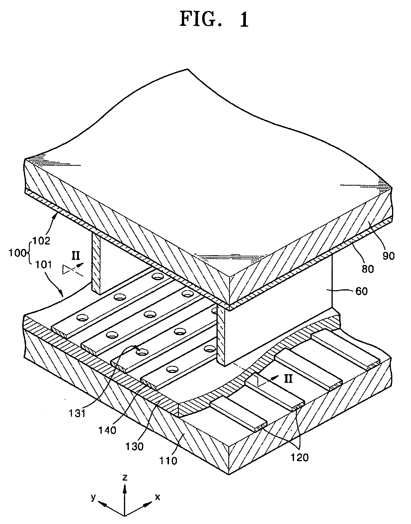
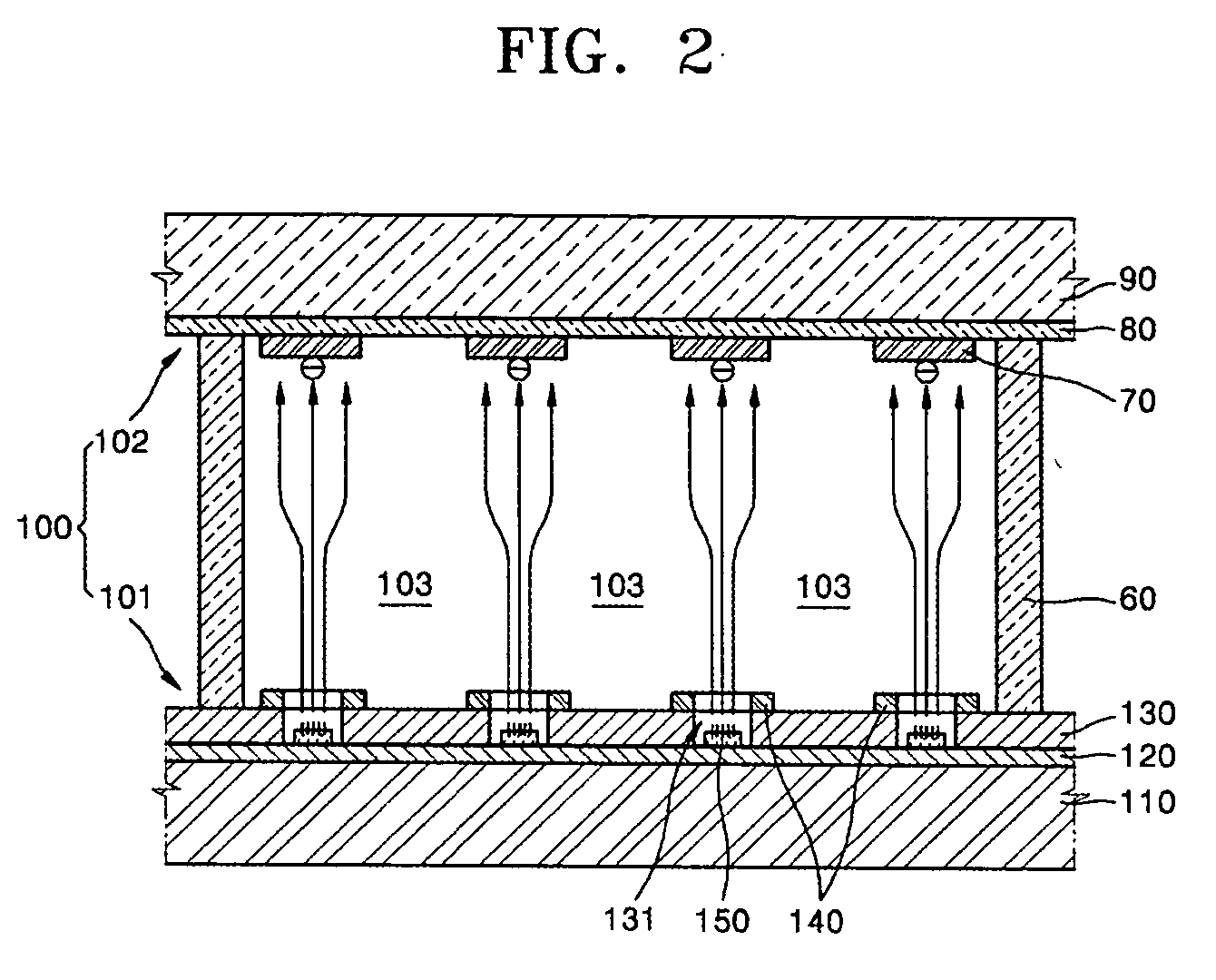
[0036]FIG. 1 illustrates a partial perspective view of a flat panel display device using an electron emission device according to the present invention and FIG. 2 illustrates a cross-sectional view taken along line II-II of FIG. 1. Referring to FIGS. 1 and 2, an electron emission display device 100 may include an electron emission device 101 and a front panel 102, which may be disposed parallel to and facing each other. A plurality of spacers 60 may be provided in order to maintain a gap between the electron emission device 101 and the front panel 102, the gap defining a vacuum space 103.
[0037] The electron emission device 101 may include a first substrate 110, a plurality of gate electrodes 140 and cathode electrodes 120 on the first substrate 110, and an insulating layer 130 interposed between the gate electrodes 140 and the cathode electrodes 120 to electrically insulate the gate electrodes 140 from the cathode electrodes 120. The gate electrodes 140 and the cathode electrodes 12...
second embodiment
[0070]FIG. 5 illustrates a cross-sectional view of an electron emission device according to the present invention. Referring to FIG. 5, an electron emission device 201 may include a second insulating layer 135 and a focusing electrode 145 in addition to the substrate 110, the cathode electrode 120, the gate electrode 140, the insulating layer 130 and the electron emission source 150 included in the electron emission device 101 (refer to FIGS. 1 and 2).
[0071] The focusing electrode 145 may be insulated from the gate electrode 140 by the second insulating layer 135 and may focus electrons that are emitted from the electron emission source 150 by the electric field formed between the gate electrode 140 and the cathode electrode 120. The electron emission of the electron emission device 201 with the focusing electrode 145 may be significantly increased when the electron emission material having a thermal electron emission layer according to the present invention is used in the electron ...
third embodiment
[0072]FIG. 6 illustrates a partial cross-sectional view of a flat panel display device and an electron emission device according to the present invention. Referring to FIG. 6, the flat panel display device 3 may include an electron emission device 2 and a front panel 1. The front panel 1 may include the second substrate 90, and the anode electrode 80 and the phosphor layer 70 formed on a lower surface of the front substrate 90. The phosphor layer may be formed on the anode electrode 80, as illustrated, or, in another implementation, may be formed under the anode electrode 80 (not shown).
[0073] The electron emission device 2 may include a first substrate 10 disposed in parallel to and facing the second substrate 90, at least one cathode electrode 20 formed in a striped pattern on the first substrate 10, at least one gate electrode 30 formed in a striped pattern parallel to the cathode electrode 20, and electron emission layers 40 and 50 that respectively surround the cathode electrod...
PUM
 Abstract
Description
Claims
Application Information