Dual port semiconductor memory device

a memory device and semiconductor technology, applied in semiconductor devices, digital storage, instruments, etc., can solve the problems of limited operation speed of single-port sram devices and affect the operation speed of sram devices, so as to reduce parasitic capacitance, prevent crosstalk, and enhance the noise margins of memory cells

Active Publication Date: 2007-02-01
SAMSUNG ELECTRONICS CO LTD
View PDF9 Cites 10 Cited by
  • Summary
  • Abstract
  • Description
  • Claims
  • Application Information

AI Technical Summary

Benefits of technology

[0016] It is therefore an object of the present invention to address disadvantages associated with prior semiconductor memory devices. It is another an object of the present invention to provide a dual port semiconductor memory device capable of enhancing noise margins of memory cells, minimizing parasitic capacitance caused by pairs of bitlines, and preventing crosstalk between adjacent pairs of bitlines.

Problems solved by technology

The number of data read or write ports, also affects operation speed of SRAM devices.
For these reasons, operation speed of single port SRAM devices is limited.

Method used


Image

  • Dual port semiconductor memory device
  • Dual port semiconductor memory device
  • Dual port semiconductor memory device

Examples


Embodiment Construction

[0027] It should be understood that the description of this preferred embodiment is merely illustrative and that it should not be taken in a limiting sense. In the following detailed description, several specific details are set forth in order to provide a thorough understanding of the present invention. It will be obvious, however, to one skilled in the art that the present invention may be practiced without these specific details.

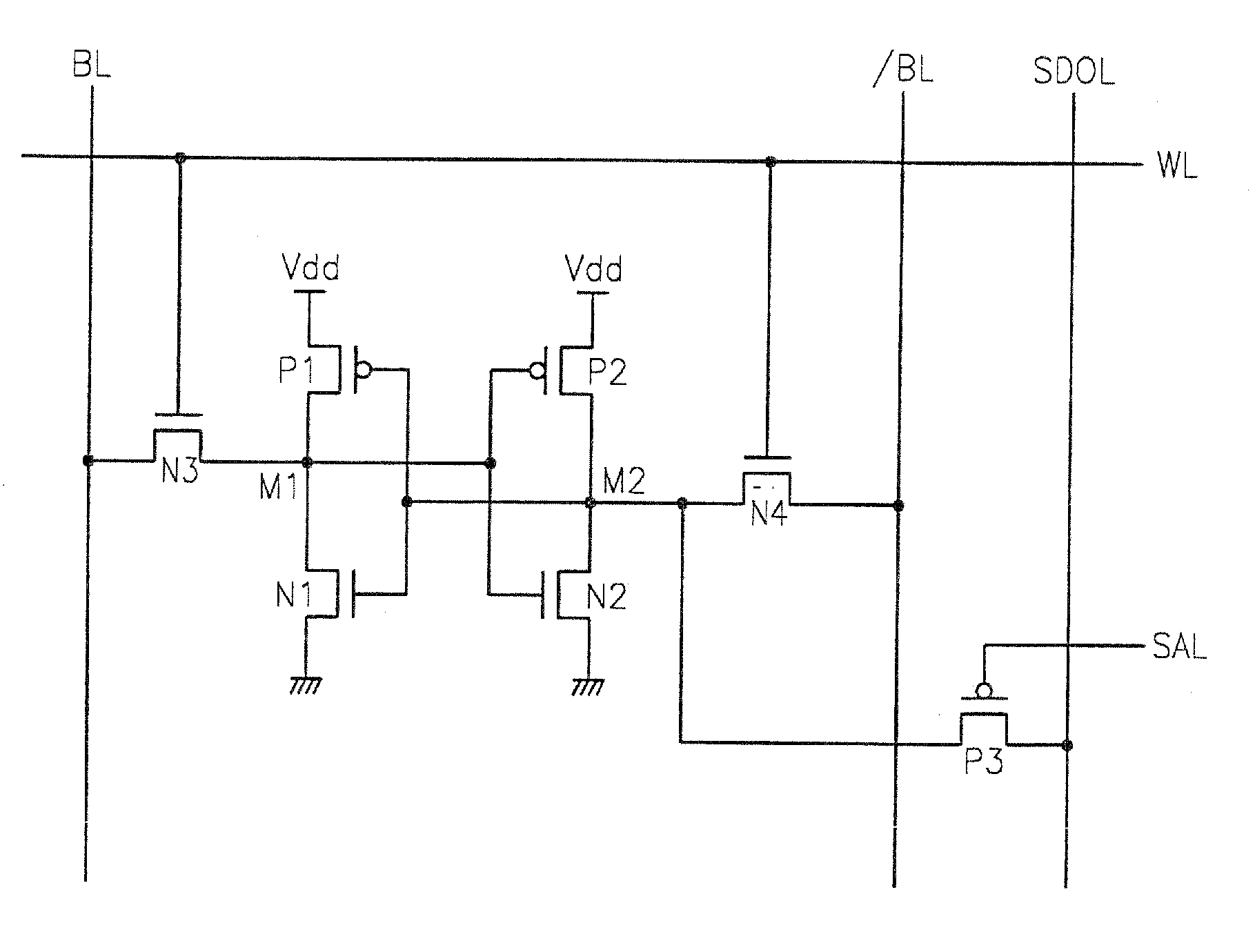
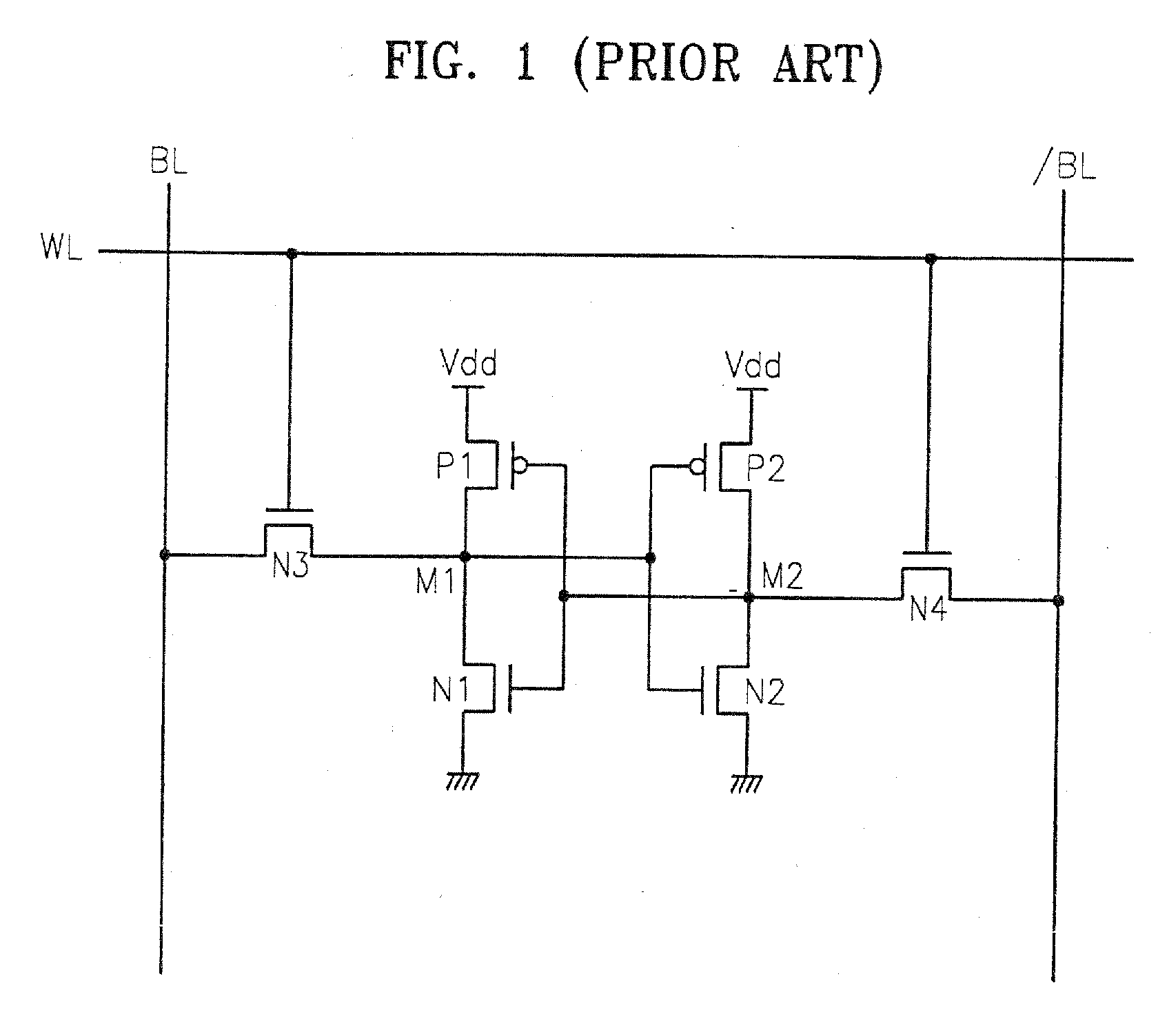
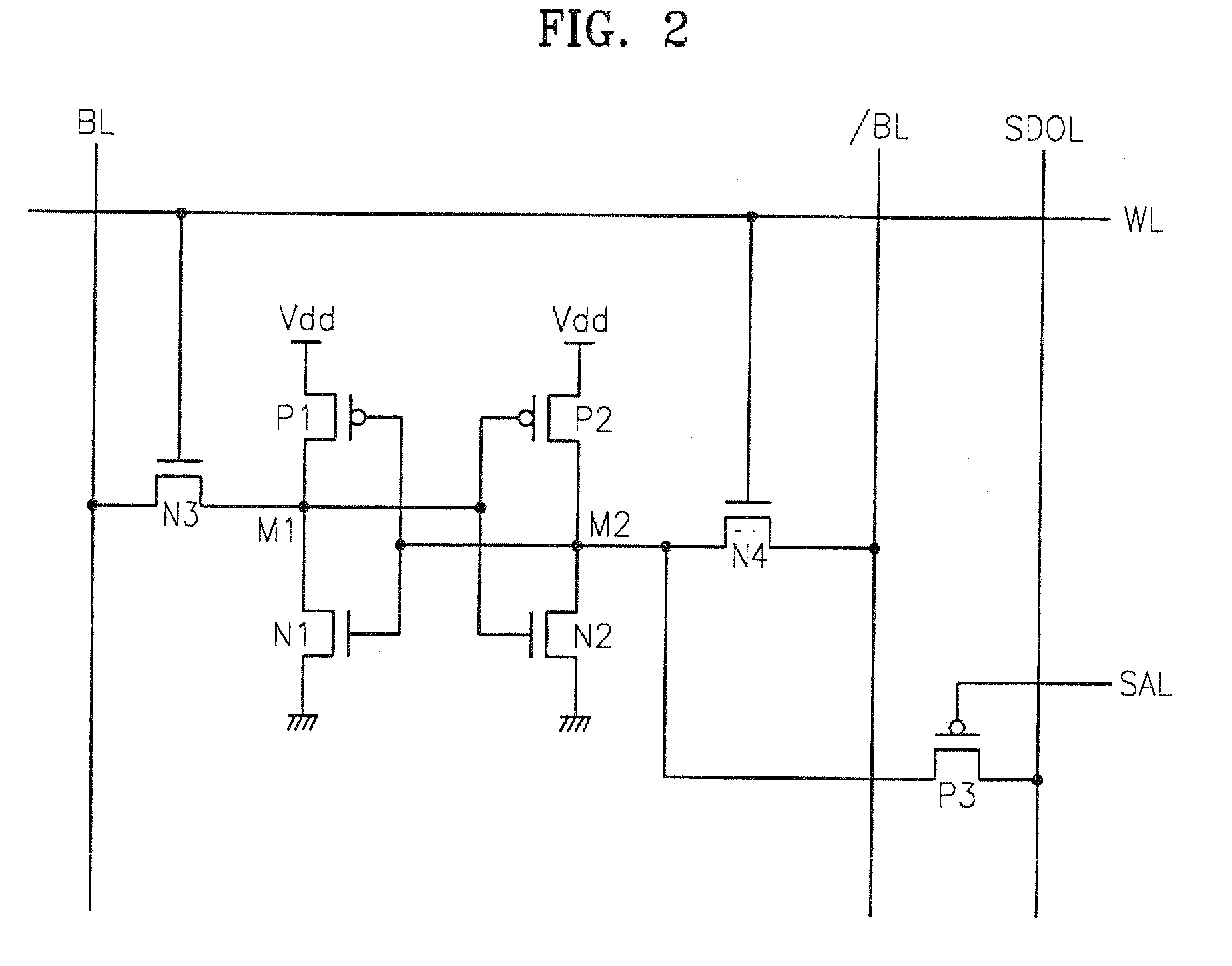
[0028] Referring to FIG. 2, a circuit diagram of a dual port semiconductor memory device according to one embodiment of the invention is disclosed. A first PMOS transistor P1 and a first NMOS transistor N1 constitute a first CMOS inverter, and a second PMOS transistor P2 and a second NMOS transistor N2 constitute a second CMOS inverter. An output port of the first CMOS inverter and an input port of the second CMOS inverter are connected, and an input port of the first CMOS inverter and an output port of the second CMOS inverter are connected. Therefore, ...


PUM


Abstract

A dual port semiconductor memory device, including PMOS scan transistors, is provided. The dual port semiconductor memory device includes two PMOS transistors, two NMOS pull-down transistors, two NMOS pass transistors, and a PMOS scan transistor. The scan transistor being PMOS, noise margins can be improved. In addition, these seven transistors are arranged in two n-wells and 2 p-wells, while n-wells and p-wells are arranged in series and in alternating fashion. Therefore, the length of a memory cell along the minor axis of the memory cell is relatively short. This memory cell layout helps shorten the length of a bit line by arranging a pair of bitlines in parallel with well boundaries, i.e., in the direction of the short axis of the memory cell, and makes it possible to prevent crosstalk between a bitline and a complementary bitline by arranging conductive lines between the bitline and the complementary bitline.

Description

BACKGROUND OF THE INVENTION [0001] This application is a Divisional of U.S. patent application Ser. No. 10 / 751,178, filed on Jan. 2, 2004, now pending, which claims priority from Korean Patent Application No. 2003-06365, filed on Jan. 30, 2003 in the Korean Intellectual Property Office, the disclosures of which are incorporated herein in their entirety by reference. [0002] 1. Field of the Invention [0003] The present invention relates to a semiconductor memory device and, more particularly, to a dual port static random access memory (SRAM) device having a memory cell comprised of a plurality of transistors. [0004] 2. Description of the Related Art [0005] Semiconductor memory devices are classified into dynamic random access memories (DRAMs) and static random access memories (SRAMs). SRAMs advantages include high operation speed, low power consumption, and simple operation. In addition, there is no need to refresh data stored in SRAMs. Since SRAMs are compatible with a logic semicond...

Claims


Application Information

Patent Timeline
Patent Type & Authority Applications(United States)
IPC IPC(8): G11C8/00G09G3/36G11C11/41G11C5/02G11C7/02G11C7/18G11C8/16G11C11/412H01L21/8244H01L27/11
CPCG09G3/3611G11C7/02H01L27/1104G11C11/4125H01L27/11G11C8/16H10B10/00H10B10/12G11C5/02
Inventor LEE, TAE-JUNGKIM, BYUNG-SUNLEE, JOON-HUNG
Owner SAMSUNG ELECTRONICS CO LTD
Why Eureka
Try Eureka