
Method of manufacturing image display panel and image display panel

a technology of image display panel and display panel, which is applied in the direction of gas-filled discharge tubes, electric discharge tubes, instruments, etc., can solve the problems of lack of imaging repetition stability, slow response rate, and difficult to maintain the stability of the dispersion state, so as to improve the adhesion property and improve the adhesion. , the effect of easy removal of the image display media

Inactive Publication Date: 2007-02-08
BRIDGESTONE CORP
View PDF3 Cites 11 Cited by
  • Summary
  • Abstract
  • Description
  • Claims
  • Application Information

AI Technical Summary

Benefits of technology

[0012] An object of the first aspect of the invention is to eliminate the drawbacks mentioned above and to provide a method of manufacturing an image display panel and an image display panel manufactured according to the method mentioned above, which can improve an adhesion property between the substrate and the partition walls, obtain an excellent result even in an endurance test, and easily remove the image display media remaining on the partition walls.
[0016] An object of the second aspect of the invention is to eliminate the drawbacks mentioned above and to provide a method of manufacturing an image display panel and an image display panel manufactured according to the method mentioned above, which can improve an adhesion property between the substrate and the partition walls and obtain an excellent result even in an endurance test.
[0020] An object of the third aspect of the invention is to eliminate the drawbacks mentioned above and to provide a method of an image display panel and an image display panel manufactured according to the method mentioned above, having a rapid response due to a dry type, an inexpensive cost and an excellent stability, which can further form the partition walls in which an excellent wall pattern can be obtained since an insufficient development is not caused and in which an adhesion property to the substrate can be maintained.

Problems solved by technology

However, in the electrophoresis method, there is a problem that a response rate is slow by the reason of viscosity resistance because the particles migrate among the electrophoresis solution.
Further, there is a problem of lacking imaging repetition stability, because particles with high specific gravity of titanium oxide is scattered within solution of low specific gravity, it is easy to subside, difficult to maintain a stability of dispersion state.
Even in the case of microencapsulating, cell size is diminished to a microcapsule level in order to make it hard to appear, however, an essential problem was not overcome at all.
[The Imaging Society of Japan “Japan Hardcopy '99” (Jul. 21-23, 1999) Transaction Pages 249-252] However, the structure becomes complicated because the charge transport layer and further a charge generation layer are to be arranged.
In addition, it is difficult to constantly dissipate charges from the electro-conductive particles, and thus there is a drawback on the lack of stability.
However, there is a drawback such that an adhesion property to the glass used as the substrate is not sufficiently obtained if using the hot-melt adhesive or the reaction type hot-melt adhesive.
As a result, in various endurance tests (heat-resistant test, humidity test), there is a drawback such that the adhesion property is decreased remarkably.
Moreover, if using such liquid-like adhesives, there is a drawback such that the image display media remaining on the partition walls can not be removed due to the adhesive on the partition walls in the case of filling the image display media between the partition walls (tasks of a first aspect of the invention).
In this case, since a washing with respect to the substrate and the partition walls before applying the adhesive is not sufficient, there is a drawback such that a sufficient adhesion property can not be obtained.
However, among the techniques mentioned above, in the case that the overall portion of the partition walls is made to a color of one of the image display media, especially in the case that the overall portion of the partition walls is formed by a dark color such as black, if a pigment or a dye having a dark color such as black is blended in the resist, there occurs a drawback such that a light transmission property of the resist used for forming the partition walls is deteriorated.
In this manner, if a light transmission property of the resist is deteriorated, there are drawbacks: such that a light is not evenly exposed to a portion at which the partition walls are to be formed by exposing and curing, when the exposure is performed through the mask; such that a possibility for causing a insufficient development, in which the partition walls are not formed according to the pattern, becomes high especially when forming high partition walls; and such that a sufficient adhesion property between the formed partition walls and the substrate can not be obtained (tasks of a third aspect of the invention).

Method used


Image

  • Method of manufacturing image display panel and image display panel
  • Method of manufacturing image display panel and image display panel
  • Method of manufacturing image display panel and image display panel

Examples


embodiment

[0106] Then, examples and comparative examples are shown so as to explain the present invention further specifically. However, the present invention is not limited to the following examples and comparative examples.

[0107] [As to the First Aspect of the Invention]

example 1

[0108] The partition walls 4 each having an opening portion of 300 μm□, a line width of 100 μm and a height of 100 μm were formed on an ITO glass substrate of 30 Ω / □ (corresponding to the front substrate 1, t=0.7 mm) by means of a photo-resist method so as to obtain the electrode substrate with the partition walls 11. Moreover, the adhesive mixture was obtained by mixing 10 g of TB3052 by Three Bond Co., Ltd., as the photo-curing resin and 10 g of TB2202 by Three Bond Co., Ltd., as the heat-hardening resin. Then, as shown in FIG. 4a, the adhesive mixture was applied on the partition walls 4 by using the roll coater method so as to form the adhesive layer 12.

[0109] Then, as shown in FIG. 4b, an ultraviolet light was irradiated to the adhesive layer 12 under 1000 mJ / cm2 by using a high pressure mercury lamp so as to slightly harden the adhesive layer 12. Then, as shown in FIG. 4c, 6 g / m2 of the white particles 3W and 6 g / m2 of the black particles were filled in the cells 13 by using ...

example 2

[0112] The image display panel was manufactured as is the same as the example 1 except that 10 g of TB2210 by Three Bond Co., Ltd., was used as the heat-hardening resin and the conditions of the heat press were at 90° C. for 60 minutes under 10 MPa, and the estimate of the manufactured image display panel was performed as is the same as the example 1. The results are shown in the following Table 1.


PUM


Abstract

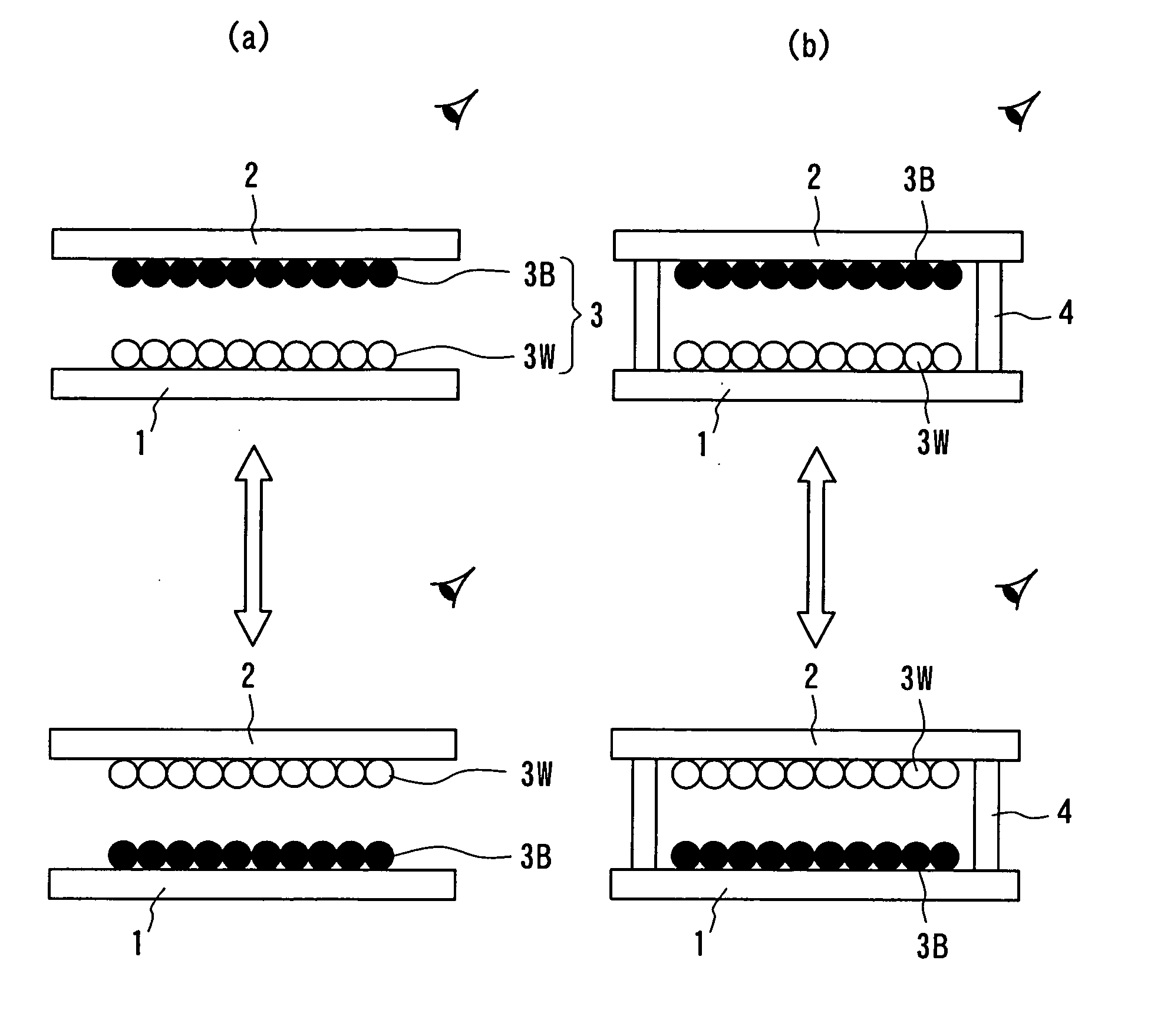
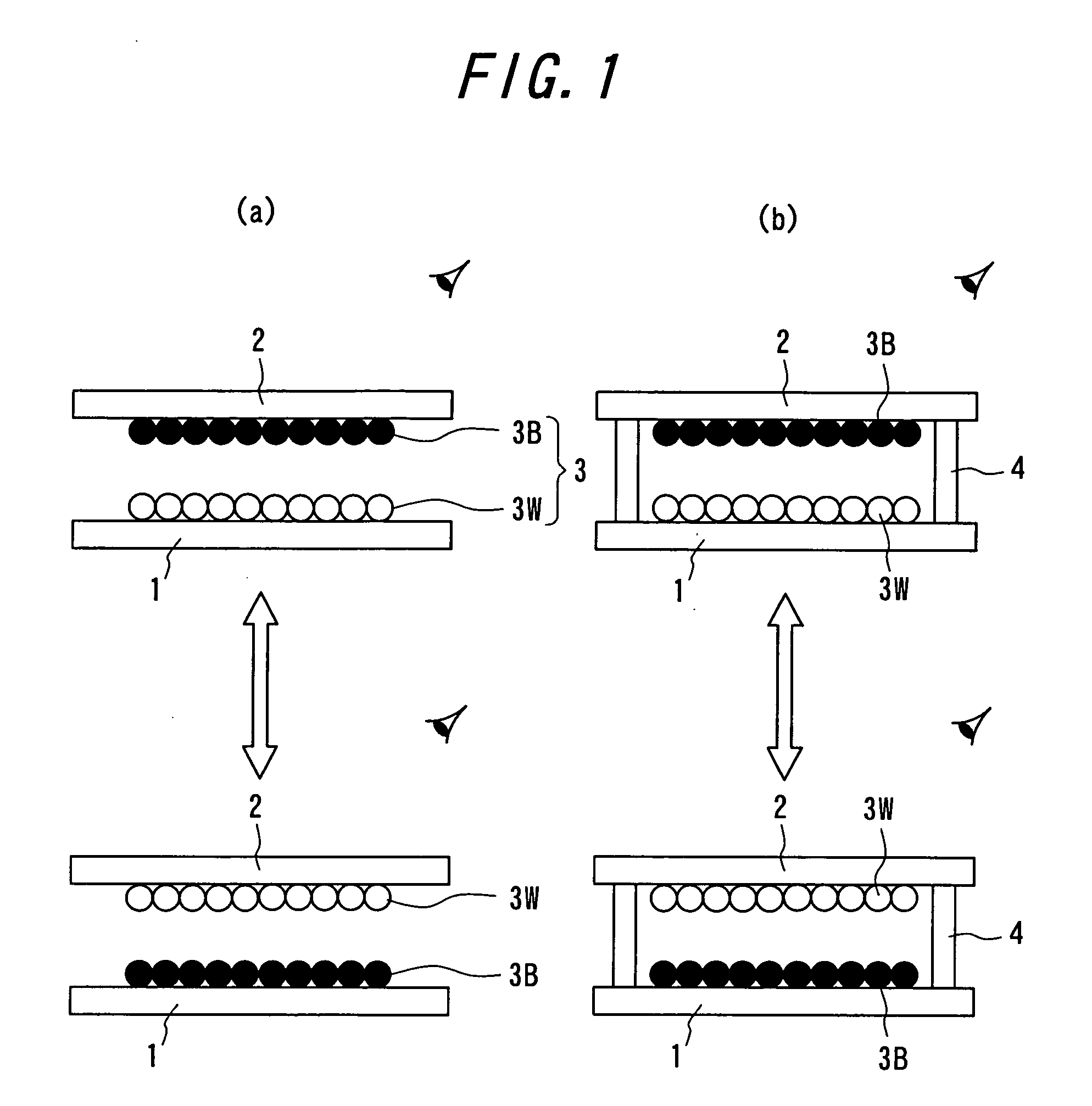
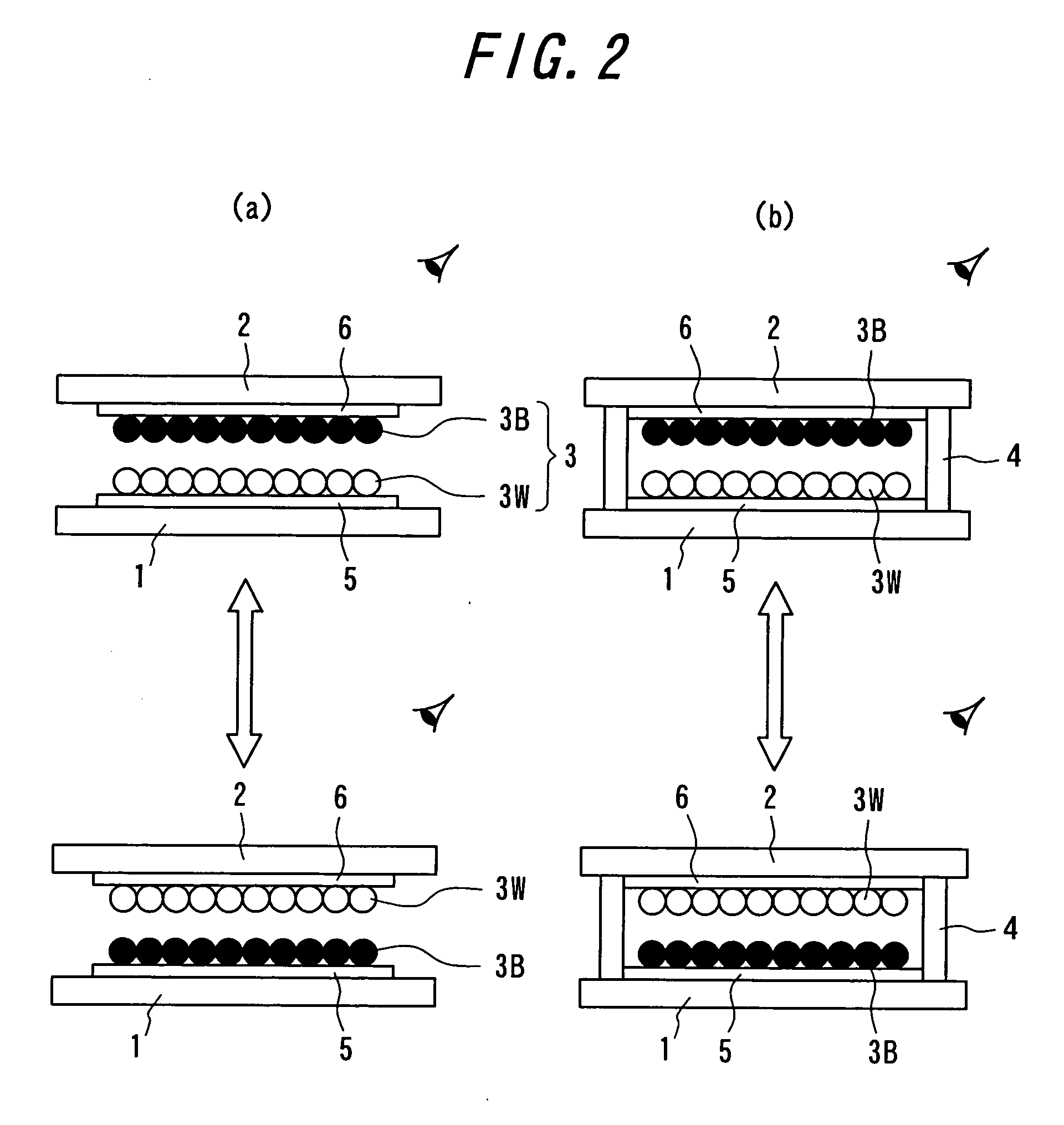
A method of manufacturing an image display panel, having one or more cells formed in an isolated manner from one another by partition walls and accommodating image display media and a plurality of image display elements, in which the image display media are sealed between opposed two substrates, at least one of the two substrates being transparent, and, in which the image display media, to which an electrostatic field is applied, are made to move so as to display an image, characterized in that the improvement comprises the steps of: (1) manufacturing a substrate with the partition walls on one substrate; applying an adhesive mixture obtained by mixing a photo-curing resin and a heat-hardening resin on the partition walls; and then connecting the other substrate to the partition walls through the adhesive mixture, the steps of: (2) manufacturing a substrate with the partition walls by forming the partition walls on one substrate; performing a washing by a dry treatment with respect to the thus manufactured substrate with the partition walls; applying an adhesive on the partition walls; and connecting the other substrate to the partition walls through the adhesive, or the steps of: (3) manufacturing the partition walls on one substrate by means of a pale color resist; applying an adhesive colored by a dark color on the partition walls; and connecting the other substrate to the partition walls through the adhesive.

Description

TECHNICAL FIELD [0001] The present invention relates to a method of manufacturing an image display panel and an image display panel, in which an image can be displayed or deleted repeatedly by moving an image display media (particles or liquid powders) by means of electrostatics. BACKGROUND ART [0002] As an image display device substitutable for liquid crystal display (LCD), image display devices with the use of technology such as an electrophoresis method, an electro-chromic method, a thermal method, dichroic-particles-rotary method are proposed. [0003] As for these image display devices, it is conceivable as inexpensive visual display device of the next generation from a merit having wide field of vision close to normal printed matter, having smaller consumption with LCD, or having a memory function, and spreading out to a display for portable device and an electronic paper is expected. Recently, electrophoresis method is proposed that microencapsulate dispersion liquid made up wi...

Claims


Application Information

Patent Timeline
IPC IPC(8): H01J17/49G02F1/1333G02F1/1335G02F1/1339G02F1/1341G02F1/1679
CPCG02F1/133377G02F1/1335G02F2001/1674G02F1/1341G02F1/167G02F1/13394G02F1/1671G02F1/1679
Inventor KOBAYASHI, TAICHIHIRAOKA, HIDETOSHISHOJI, TAKANORI
Owner BRIDGESTONE CORP
Learn More